 Gee Bartlett
Finished the initial design the 64K address space is divided up as so.
0x0000-0x7FFF RAM
0x8000-0x8FFF Peripheral space
0x9000-0xFFFF ROM
I initially had the ROM at the bottom of the address space and the RAM at the to how every thanks to many people on twitter I was informed that the Reset Vector this is a memory address that contains the first address to execute code from should be contained in ROM (this is something I didn't know before this project). The Reset Vector for this MPU is 0xFFFE right at the top of the address space so the RAM and ROM got swapped.
I decided to use a 3 to 8 decoded to select the peripheral instead of basic gates The reason is if i want to add a display buffer or other device i could take a lead form that sacrificing 4K of ROM space.
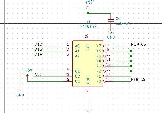
_A15 is the inverse to A15 generated by a FET and pull-up resistor so it goes low when A15 is high. I also needed it to select between this and the RAM at the bottom of the address space.
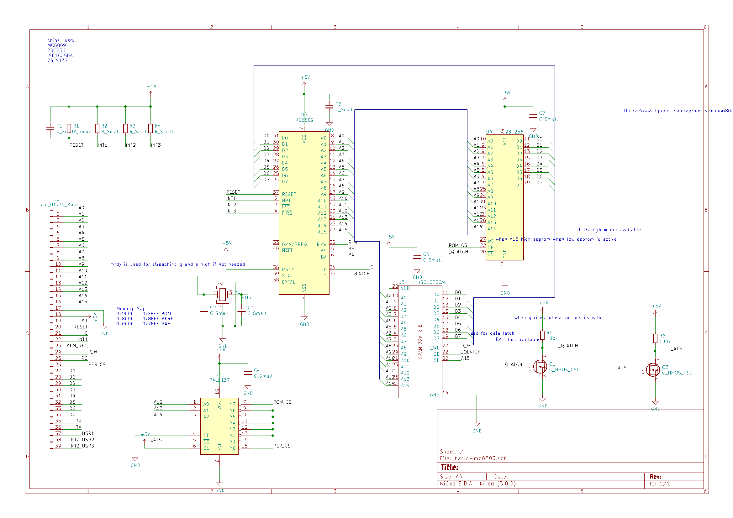
This the full schematic have been over it several times and believe cleaned up any issues.
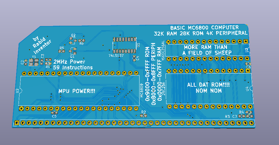
This is board almost as it has been sent off to the board house I did some more trace optimizing and managed to remove a load of vias.
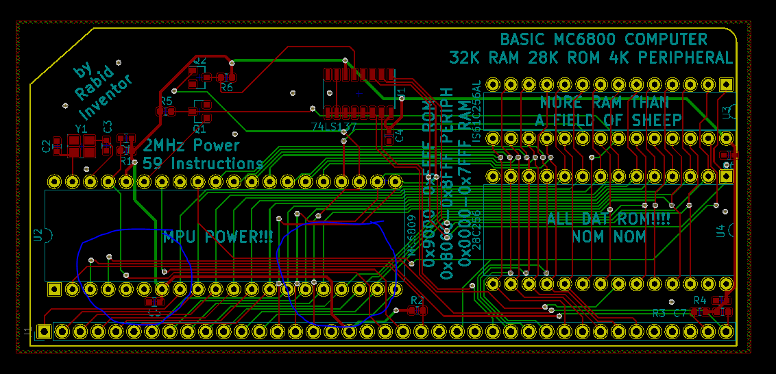
As you see in the area I have marked in blue.
So now the PCBs are ordered with JLCPCB so just a waiting game.
wish me luck :)
Discussions
Become a Hackaday.io Member
Create an account to leave a comment. Already have an account? Log In.