So.......
As pointed out here and on twitter I have my decode logic for the ROM and Peripheral addressing a but wrong.
well blue magic smoke kind of wrong :D
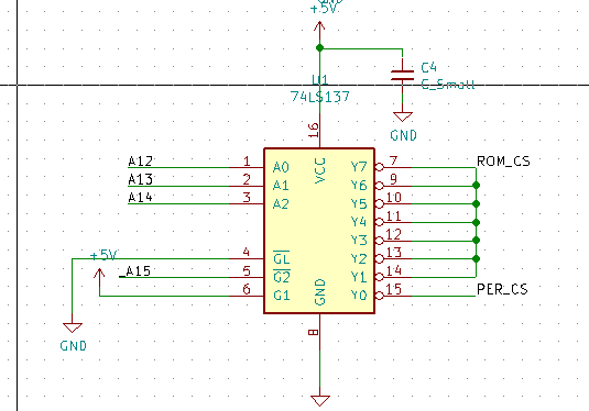
this circuit

would mean that if any of Y7 to Y1 are active then it would sink the the current from the rest. The high state of each gate is provided by a 120ohm resistor this means, 6 x 40mA would sink into the active gate.
There is not really a way to bodge this well so on this pin of the board i am going to hardware _A15 to ROM _CS or maybe do something else of board.
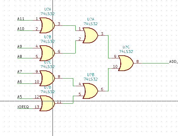
I'm experimenting with ideas but i think my final solution will look something like this.

using multiple OR gates to drive the select line. I this format I think the select will be low only if every input is off. this is taken from the IO board I am currently working on.
Let me know what you think......
 Gee Bartlett
Discussions
Become a Hackaday.io Member
Create an account to leave a comment. Already have an account? Log In.