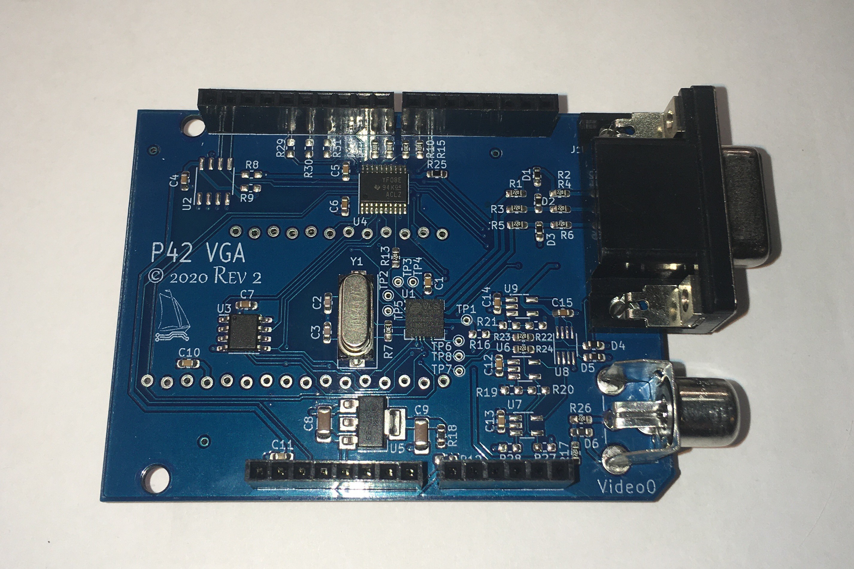
Revision 2 of the board is running as planned. I replaced the trusted level shifter buffer 74LVC4245A with a TI TXS0108, which is automatically bi-directional. The bi-dir feature is not needed here, but a good exercise for future use. Attention has to be paid, as there is also a TXB010x family which works better with fully driven signals. The TXS0108 is on order for open drain signals, e.g. the MISO sinal on SPI slave devices.

Channel 0 is on the RCA connector, channels 1,2,3 are on the VGA connector, accessible with a VGA to 3x RCA cable.
 MagicWolfi
Discussions
Become a Hackaday.io Member
Create an account to leave a comment. Already have an account? Log In.
@Thomas Yes, a clean ground plane is the ideal case, which is unfortunately almost impossible on a 2-layer board with sufficient complexity. Looking not only at the signal but also the return current is my standard approach for those cases. Because current flows in loops, always. Either you or James Maxwell picks the return path. :)
Are you sure? yes | no
This looks nice. That's a two-sided PCB, is it?
Are you sure? yes | no
Thanks. Yes. Well, it is 2-layer board and components on 2 sides. Mostly parts on the topside, bottom side is almost all GND plane, some signal under the BGA and level shifter. I'll put up some more pictures in the gallery.
Are you sure? yes | no
There is always a trade-off when using 2-layer boards. I think that keeping the ground plane clean can become a way of thinking, a core part of the design process.
Are you sure? yes | no