On the 14th, I received my printed circuit boards for the Pixel Pusher. Yesterday, I got around to trying to build one of the three prototype boards I received.

This is what a bare board looks like, component side up.
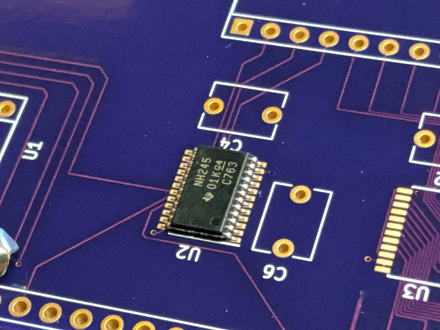
My first task is to place the highest risk components first, so as to just get them out of the way. In this case, the two 74LV8C245PWR chips, as they're incredibly small devices that even an idle breeze can cause to slip off and never be found again.
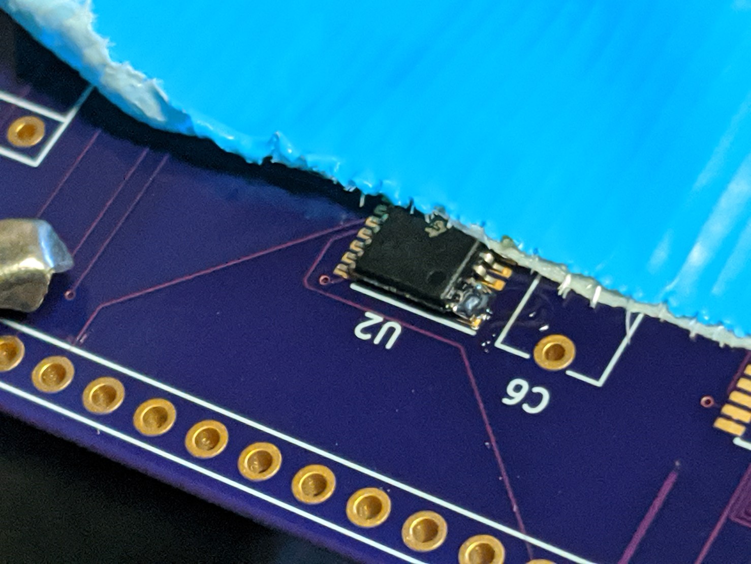
I use blue duct tape for this purpose which is not the best thing to use but it's all I had available. Tacking one corner of the chip down is sufficient to hold it in place.
PRO TIP: The ideal tape for this would have been blue painter's tape. In order to reduce the stickiness of the duct tape down to something comparable to painter's tape, I just applied and removed the duct tape strip off the work bench several times until I was comfortable with the strength of the remaining glue. The workbench was naturally dusty, so each application added more dust to the strip, which had the effect of reducing how sticky the strip was.
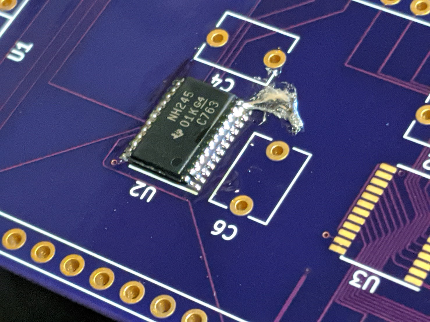
I next applied liberal amounts of solder to the chip's connections. This ensured all pins were soldered to the pads, but it also ensured that all pins were soldered to each other as well. This excess solder had to be removed. I used solder wick for this purpose.
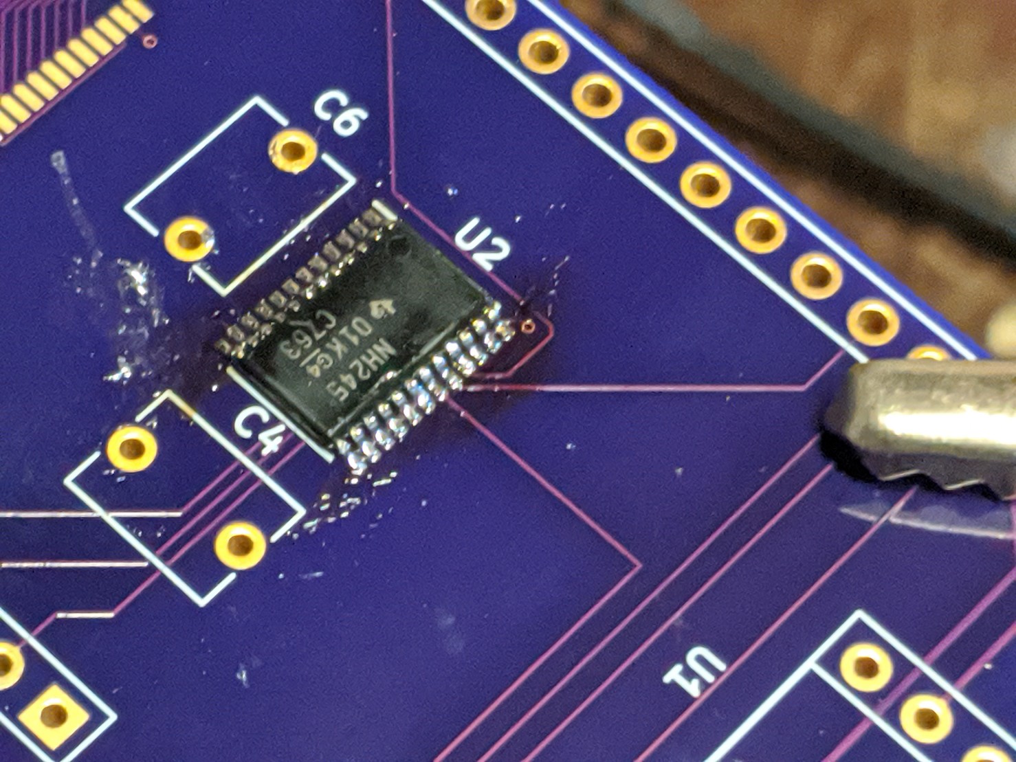
After fighting a bit with the solder wick (as evidenced by the slightly scorched flux residue), I sopped up all of the excess solder. Solder wick does not remove everything, and it happens to work out that what remains is sufficient to both hold the chip in place and to ensure good contact.
Because the contacts are so small, however, It is best to perform continuity checks with other parts of the circuit. If you need to desolder and resolder/reflow the contacts on these parts, now is the time to do it before other components are added.
I just discovered that the 3.3V supply pin of U2 is not connected to the 3.3V trace. I forgot to place a via! I'll need to add a bodge wire later.
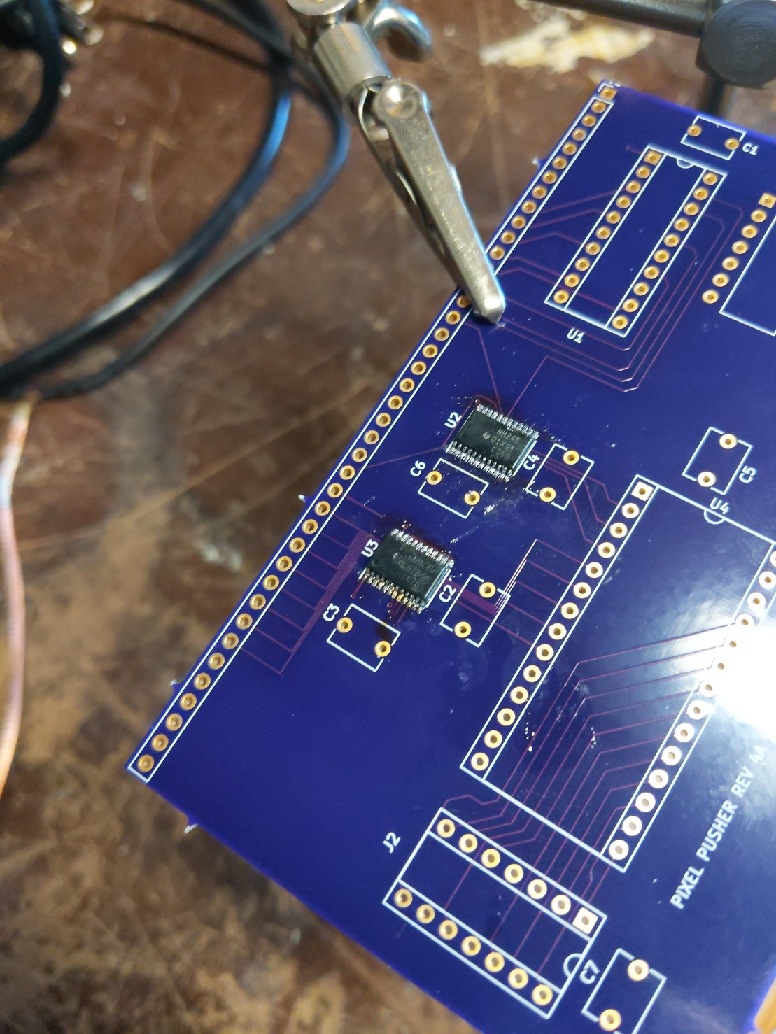
After repeating the steps above for the second level shifter chip, I'm left with a board with two nicely soldered, surface-mount chips. Thankfully, I didn't discover any more missing connections!
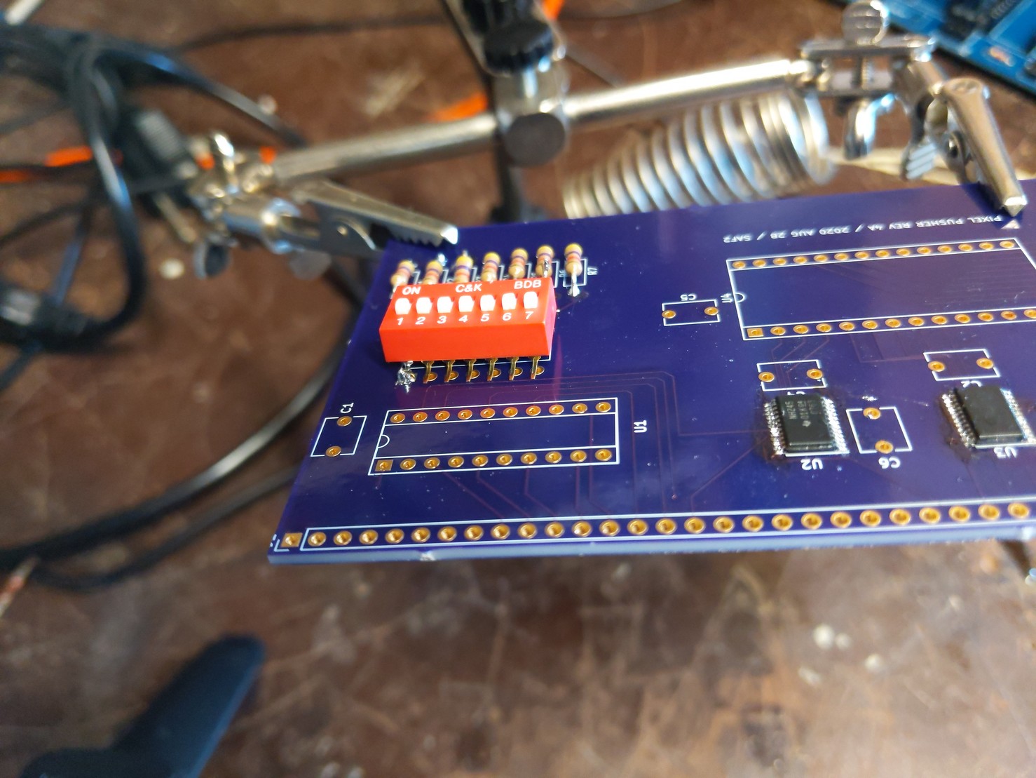
I found out the hard way that the footprint used for the DIP switches (which should have been a normal 14-pin DIP footprint) was too wide for the actual switch. Thankfully, I could splay the legs of the switch out and make surface contact with all the holes on the component-side of the board. Since all the holes are fully plated through (per OSH Park's website and as continuity checks confirm), treating the DIP switch package as a surface mount device instead of a through-hole device provides the extra length needed to ensure good contact with the rest of the circuit.
So, I splayed the pins out, tacked opposite corners of the DIP switch down, and ...
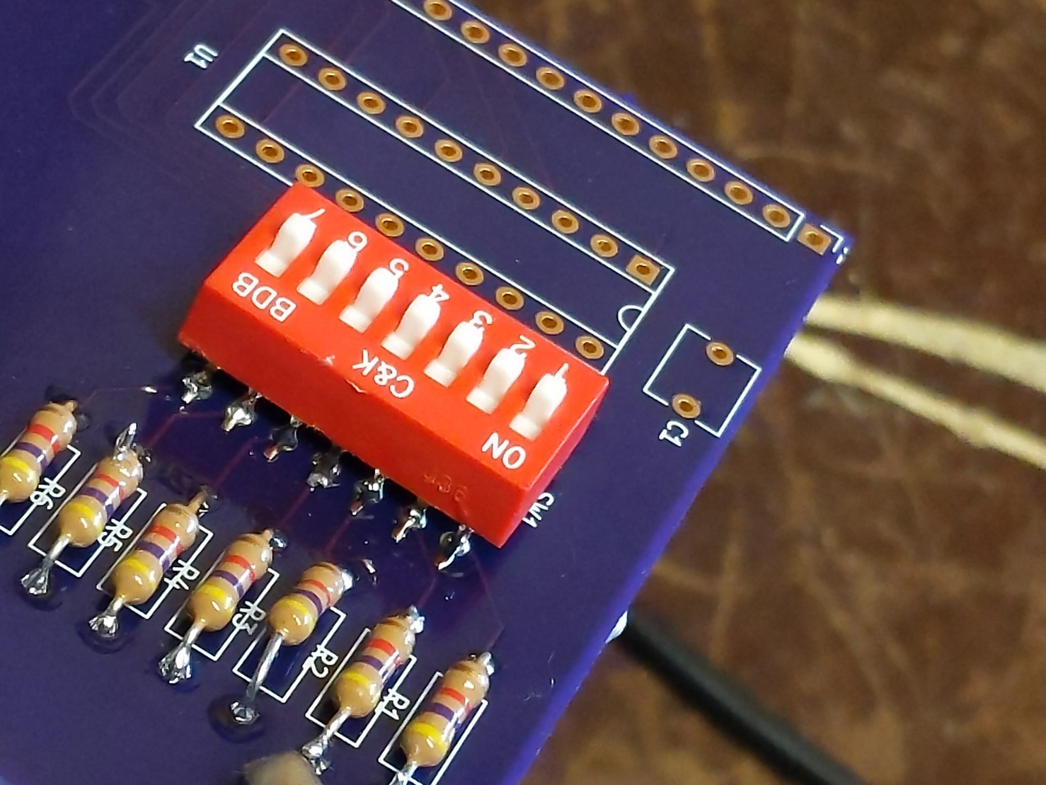
proceeded to blob solder on the remaining pins. I then set the DIP switches so that the card will respond to I/O ports 6Eh and 6Fh (not shown). I then set the DIP switches on the breadboard prototype to respond to I/O ports 6Ch and 6Dh, which would allow me to have both VDC-IIs in the RC2014 circuit at the same time without contention.
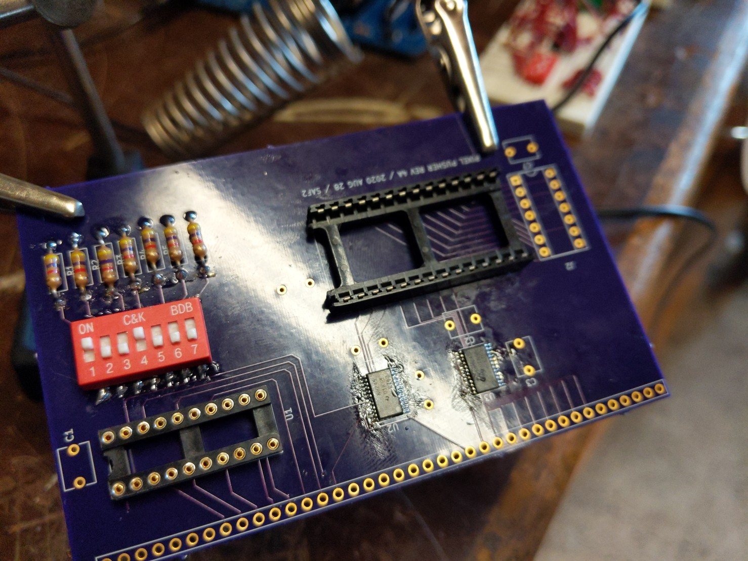
Next, I needed to fit a 28-pin, 0.6" wide socket for the TinyFPGA BX module. However, I didn't have any on-hand. Disturbing; I believe I ordered these some time ago via Amazon. Whatever, no biggie; I instead took a spare 40-pin socket I had available and chopped off six pins on either side. The result fits perfectly.
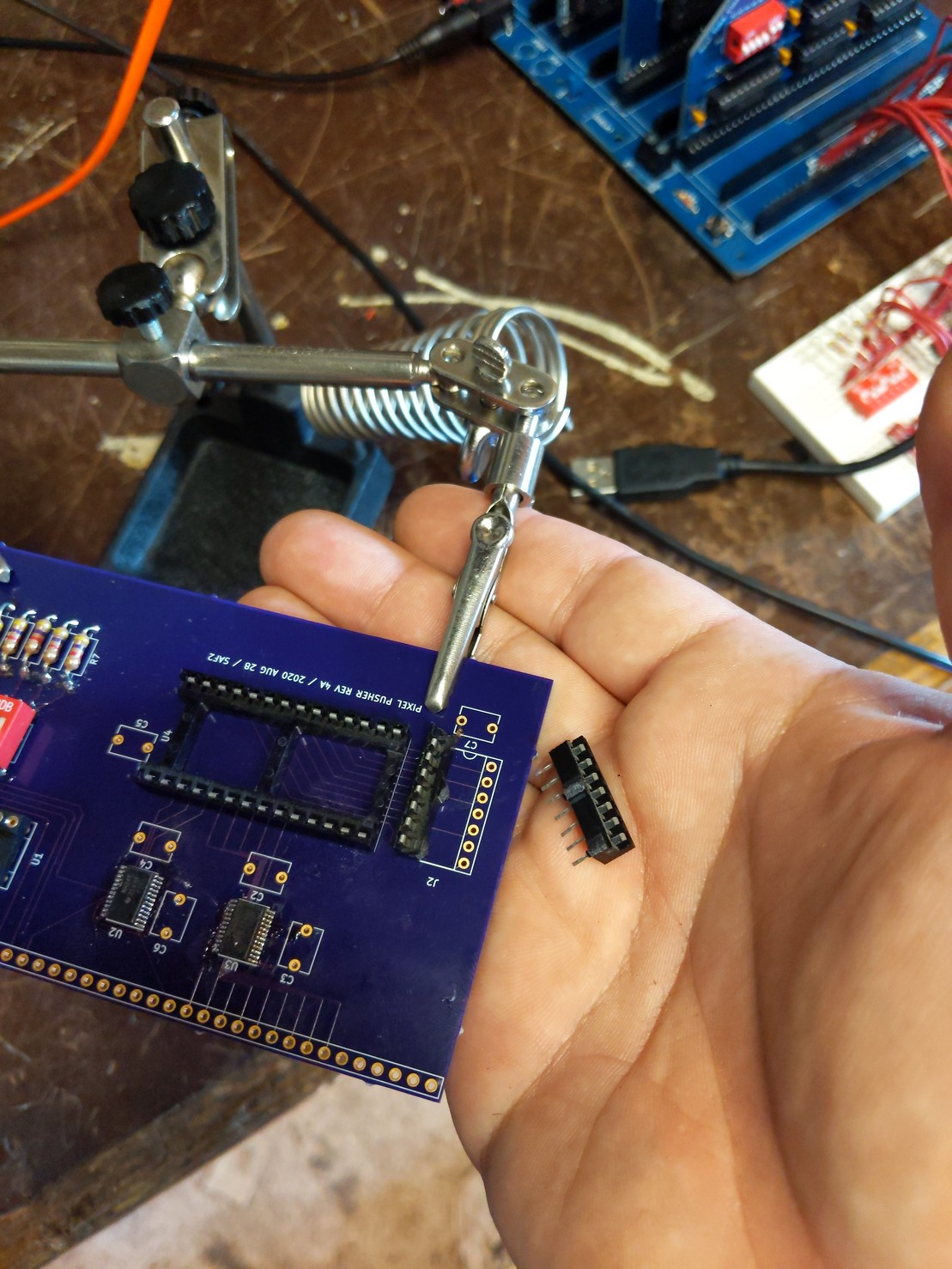
More hackery was required, as I also found out I didn't have any 14-pin DIP sockets handy either. So, I took another 0.6" wide socket (24-pin, in this case) and performed surgery on it to produce two make-shift 7-pin SIP sockets. I then placed them onto the PCB, and squeezed them together until they were 0.3" apart, roughly, which you can see below.
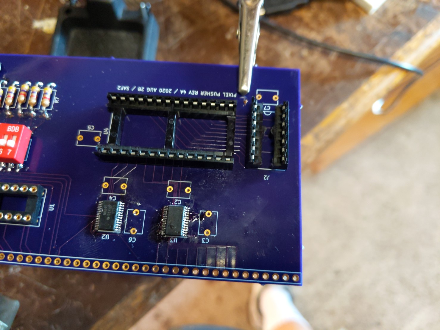
Of course, this socket is not intended to seat any chips; rather, it was intended to be used as the receptacle for a corresponding plug on a mezzanine board which included the analog bits of the interface. See my previous log entry for details on its pin-out (for video output purposes at least).
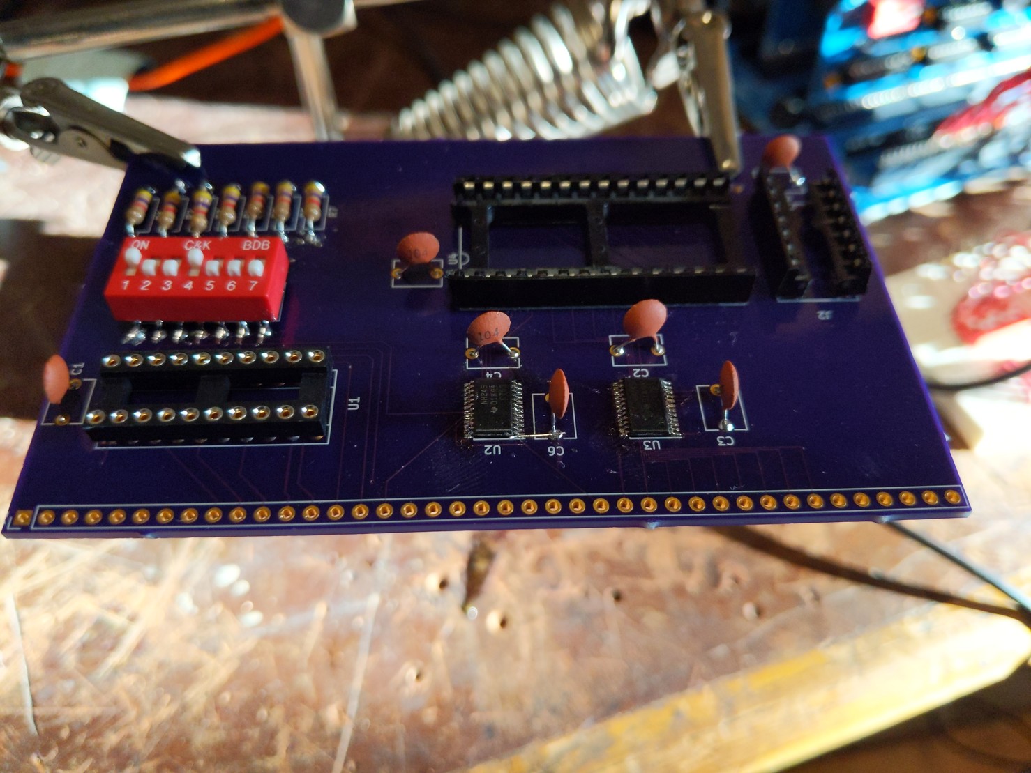
After installing the decoupling capacitors, I finally now had the means to install the bodge required to connect U2 to 3.3V supply.
This completes the soldering of the components onto the board. After soldering the 40-pin plug onto the board, the finished result looks really quite good, I must say.
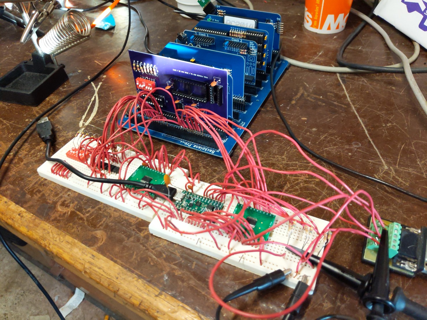
Here we see both the original breadboarded prototype of the circuit in the foreground, and immediately behind it (the only purple PCB there), we find the Pixel Pusher Revision 4A board sitting in the RC2014 backplane. These two circuits are (as far as my checks can confirm) electrically identical, so once I populate the Pixel Pusher card with a TinyFPGA BX and the 74HCT688 comparator chip, it should "just work" (where "work" is defined as the card should match the observed behavior, bug for bug and feature for feature, as the breadboarded circuit).
I ran out of time to perform testing; so, I'll need to wait until later to see how it performs.
 Samuel A. Falvo II
Discussions
Become a Hackaday.io Member
Create an account to leave a comment. Already have an account? Log In.