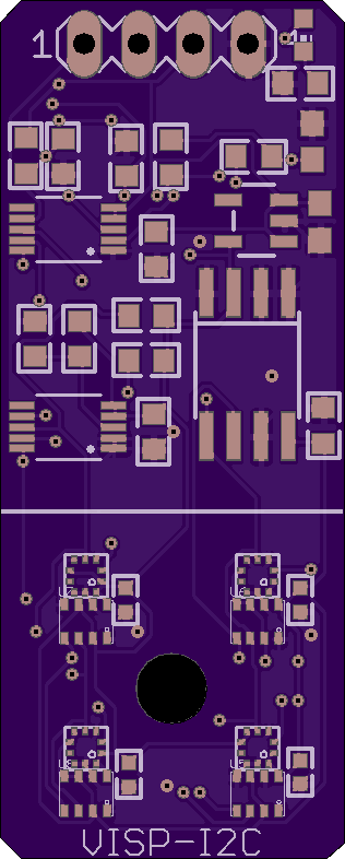
Three of the boards passed review, and were submitted to @oshpark today.
 |  |
The huge pads on the back of the sensors are for hand soldering larger bypass caps if you don't want to place the 0402 ones next to the sensors on the front.
The three solder-bridge pads labeled "Regulator Bypass" bridge across the 3.3v regulator and the I2C lines for the first translator so they can be not installed if this is to be a 3.3v only device. The first translator acts as a level shifter too for 5v operation so it makes sense to combine these.
The "ADDR" solder-bridge pads are for shifting the address of the entire device (if the first translator is installed).
Thanks to @djeddleman for reviewing the boards for us, and @Steven.Carr for making this happen!
Now, we wait.
 MasterOfNull
Discussions
Become a Hackaday.io Member
Create an account to leave a comment. Already have an account? Log In.
exciting!
Are you sure? yes | no