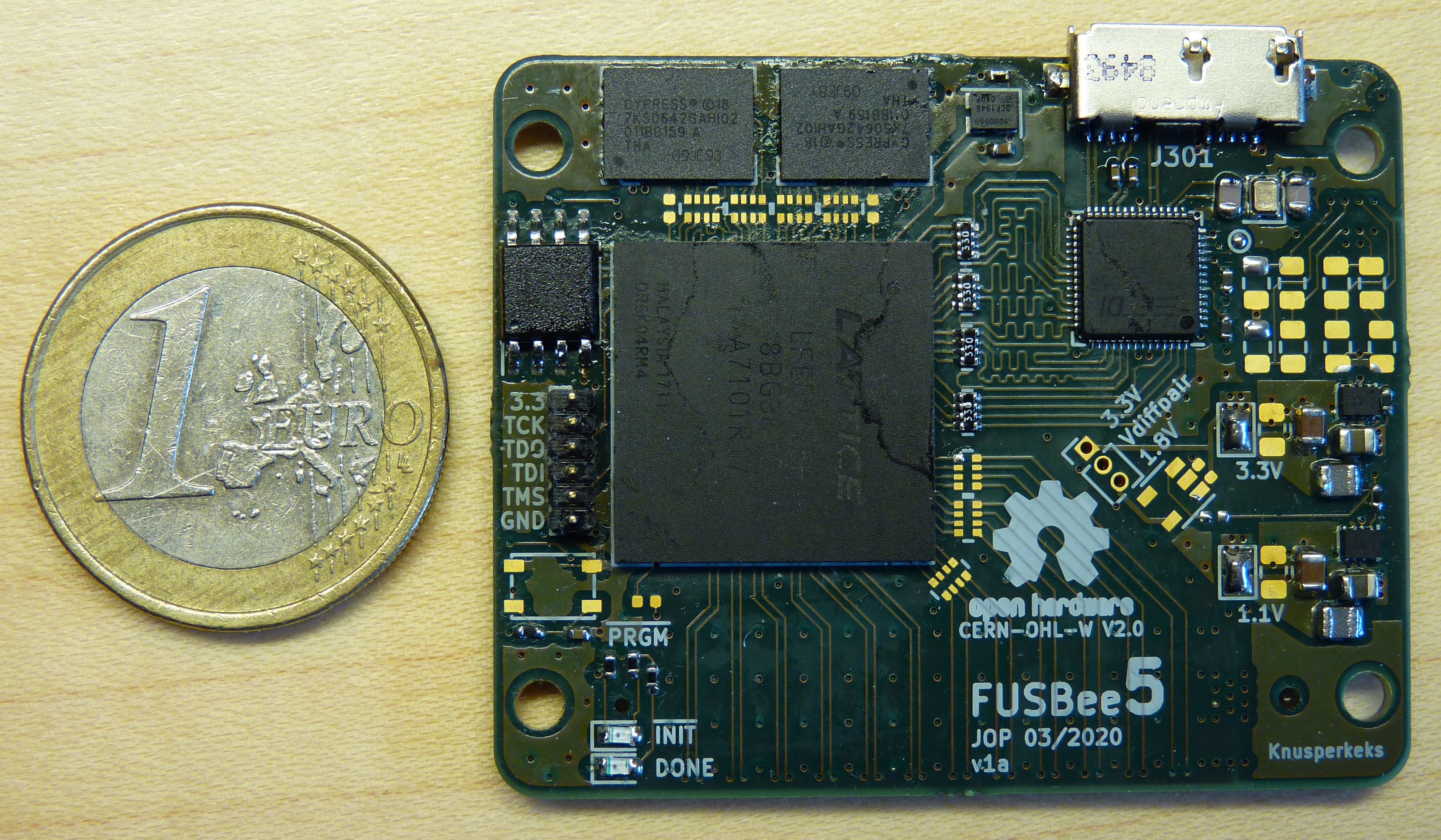
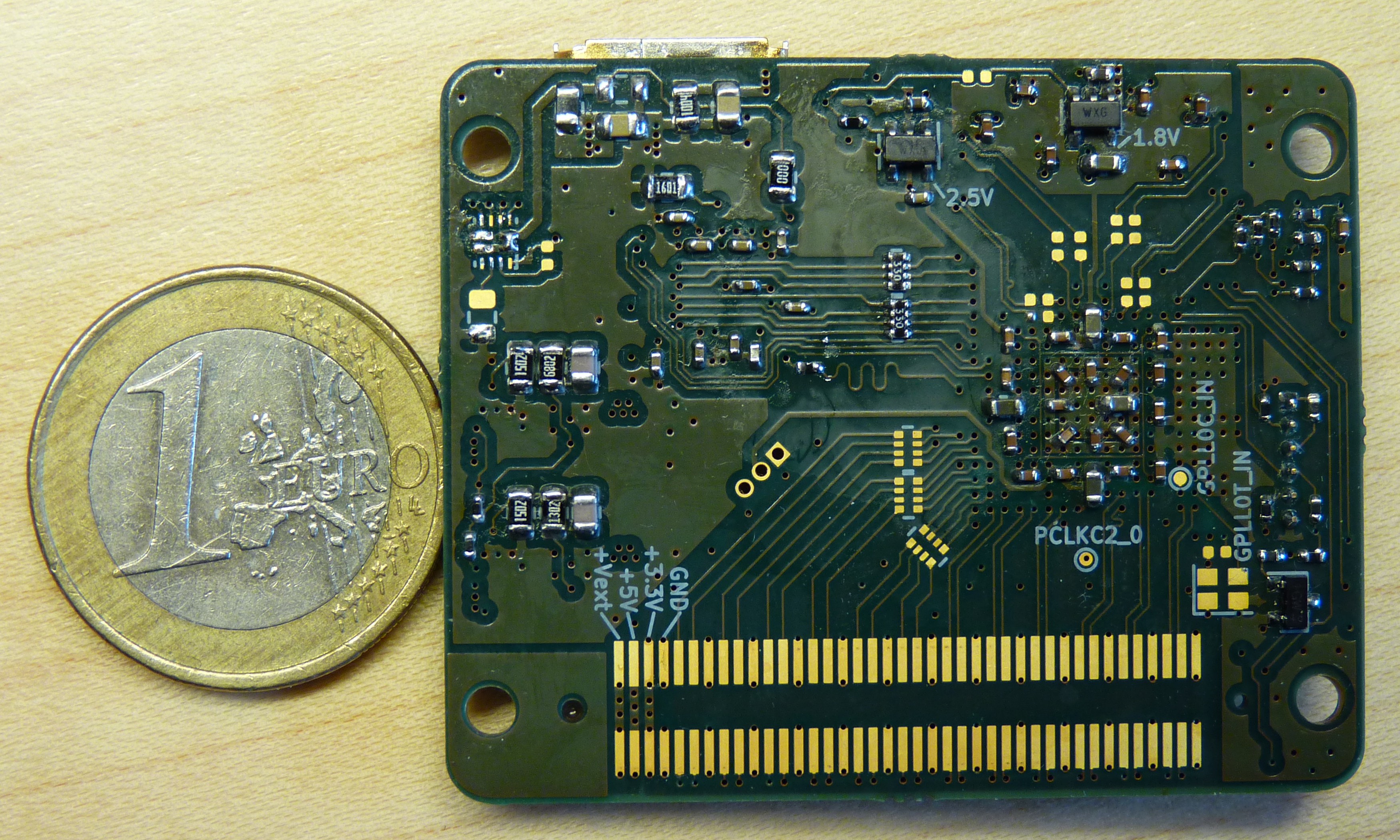
Since about two weeks, I have all parts and pcbs on hand and started building up a prototype. So far, it does look quite well and there is nothing wrong with the design! :) The overall status is:
- Most parts, except the input protection/selection circuitry, are soldered down.
- FPGA has no shorts/opens, can be programmed via JTAG and most importantly it survived my hot air torture.
- FT600 is working fine with USB2/3 and a simple loopback test from the PC to the FPGA does work fine. Just my resistor array for series termination is awful for hand soldering! Do you a favour and don't use the standard 4x0402 footprint for hand soldering (pads should be longer and not placed very close to a chip). One could argue that it is not very useful to place gigantic 0805 load caps on a tiny 2.0x1.6mm crystal...I was so sure to have the right 0603s in stock when I designed the board.
- Both buck converters (TPS62821) are working fine. The 1.1V one is only working in pulse skipping mode for higher efficiency, producing low freq. sawtooth ripple - some heavy computation is needed for the FPGA :D
Nevertheless, the ripple is about 13mVpp for both (quick measurement with an ADALM2000) which is not too bad.
A detailed measurement of ripple and current consumption should be done some day... - Hyperram is not tested.
- Configuration flash is not tested.
- Connector is not soldered down.


Now I will continue putting together some nMigen code to hopefully check the Hyperram. Once it is known to work (hopefully!), I will put up the design files along with an errata/todo list for future revisions.
Happy hardware hacking!
Knusperkeks
Discussions
Become a Hackaday.io Member
Create an account to leave a comment. Already have an account? Log In.