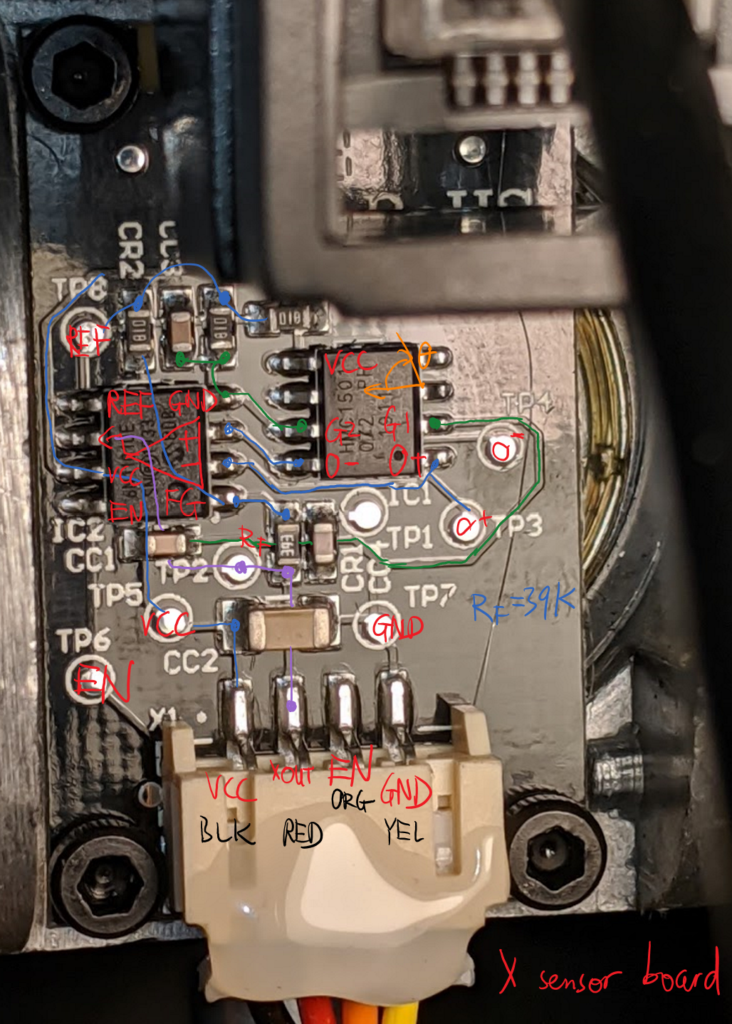
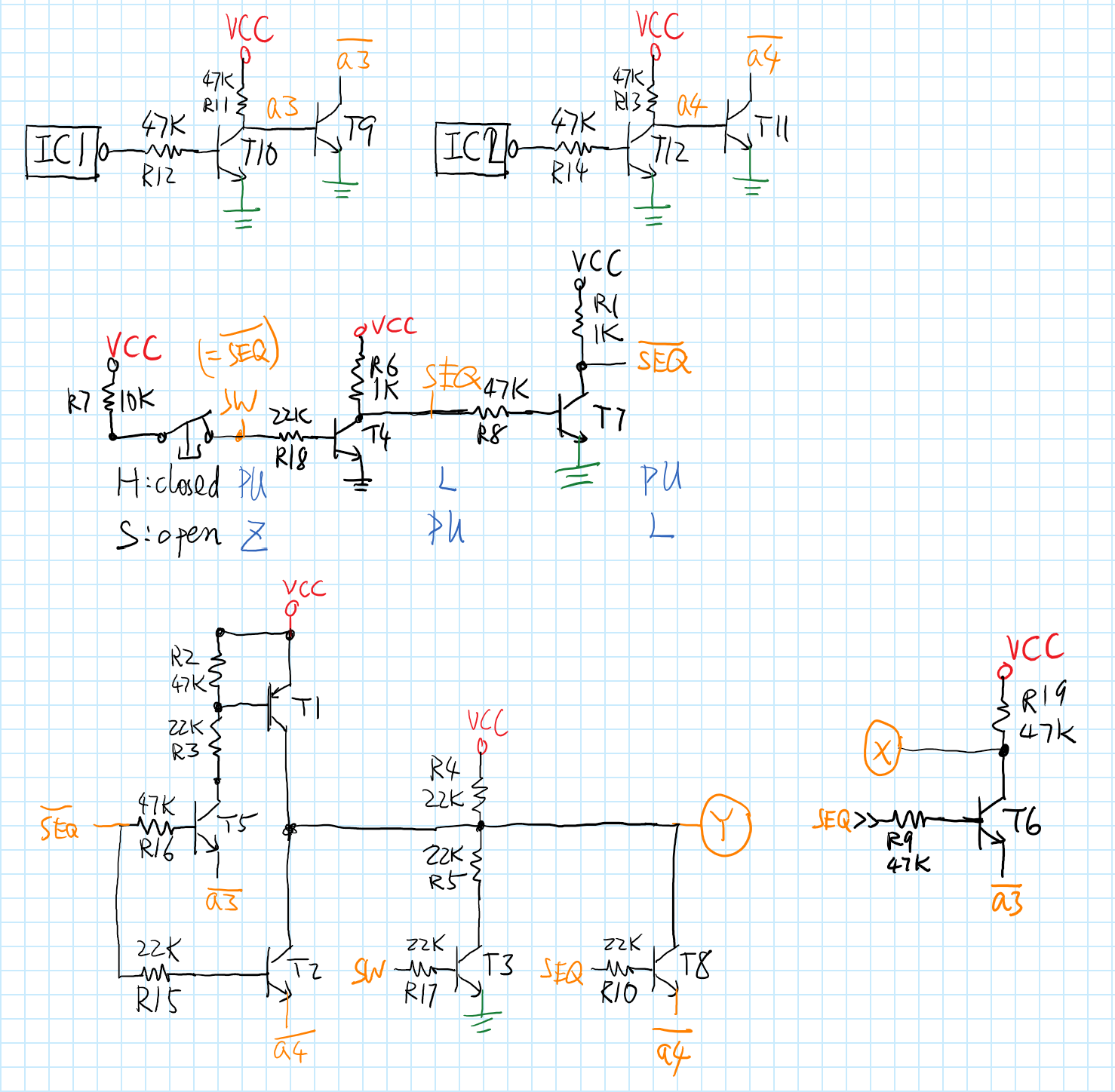
Even though it's enough to treat the shifter as a black box if the end goal is just to interface with it, curiosity took over and I decided to trace out both boards on the shifter.
X-Axis Sensor Board

This is actually very simple: HMC1501 (SOIC-8 package on the right), a magnetic encoder chip, outputs a differential voltage proportional to sin(2*theta) of a magnet rotating underneath it. This differential voltage is amplified by an instrumentation amplifier, MCP6N11-010, to its left. Reference voltage for the output is 1/2 VCC, generated with a resistor divider. The amplifier comes with an ENABLE pin --- driving it low turns the output high-Z.
Y-Axis / Main Board


This shouldn't be hard, but it tripped me up for good mainly due to its, uh, gross inefficiency.
Recall the behavior of the shifter:
- When the shifter is in H-pattern mode:
- SEQ pin is LOW
- X pin outputs X axis angle (the output from X axis board)
- Y pin is:
- VCC if lever is in R/1/3/5/7 (forward)
- 1/2 VCC if lever is in the center / neutral
- 0 if lever is in 2/4/6 (backward)
- When the shifter is in Sequential mode:
- SEQ pin is HIGH
- X pin goes LOW if the lever is pushed forward (gear 3)
- Y pin goes LOW if the lever is pulled backward (gear 4)
Let's start from each part...
Hall Effect Switches
The Y position is sensed by IC1 and IC2, both of which are SL353 hall-effect switches. These happen to have push-pull active-low output, so if a magnet is around the output is driven LOW; otherwise the output is driven HIGH. When the shifter lever is pushed forward, the magnet (right center) goes under IC1; backward, IC2.
The push-pull active-low output from each switch is put through 2 inverters (T9~12) and becomes an active-low open drain output. No other signals from this chain is used. I wonder why don't they just use a hall switch that outputs open drain in the first place; easy 4 transistors and tons of board space saved.
Mode Switch / Enable
A limit switch is connected to the 2P connector in the bottom left. It is closed in H mode, open in SEQ mode. This also went through 2 inverters. The designer sure loves his/her double inverters...
Anyway, SEQ pin is tapped off the first inverter here, while the ENABLE pin for X-axis is tapped off the second (X axis sensor enabled only in H mode).
Y axis behavior
In H mode, T3 is on, T8 is off, so R4/R5 pulls the Y pin to roughly 1/2 VCC. T5 and T2 are both on, so T1 and T2 forms a push-pull output stage, triggered by open-drain outputs from the hall switches.
In SEQ mode, T3 is off, so only R4 pulls the Y pin to VCC. T8 is on, so only IC2 open-drain output can pull the Y pin to LOW.
Surely enough, neither T2 nor T8 are necessary. Regardless of SEQ signal, IC2 open-drain output is effectively connected to the Y pin anyway.
X axis behavior
In SEQ mode, the X-axis board is disabled, and instead IC1 open-drain output can pull the X-pin.
Conclusion
Only T1,2,3,5,6 are really necessary. That's 5 out of the original 12. Both the design and layout looked grossly incompetent. Improvements would not only simplify the circuit, but also make it a lot more robust.
Why did I even waste time on this... I must have been really bored...
 Yin Zhong
Discussions
Become a Hackaday.io Member
Create an account to leave a comment. Already have an account? Log In.