The memory device flexibility results in a memory mapping problem of how to decode the memory space when the four positions each can have different chips and different memory space lengths. Having discrete logic and jumpers for the memory spaces would be extremely difficult and switching to programmable gates is a non-starter for most users.
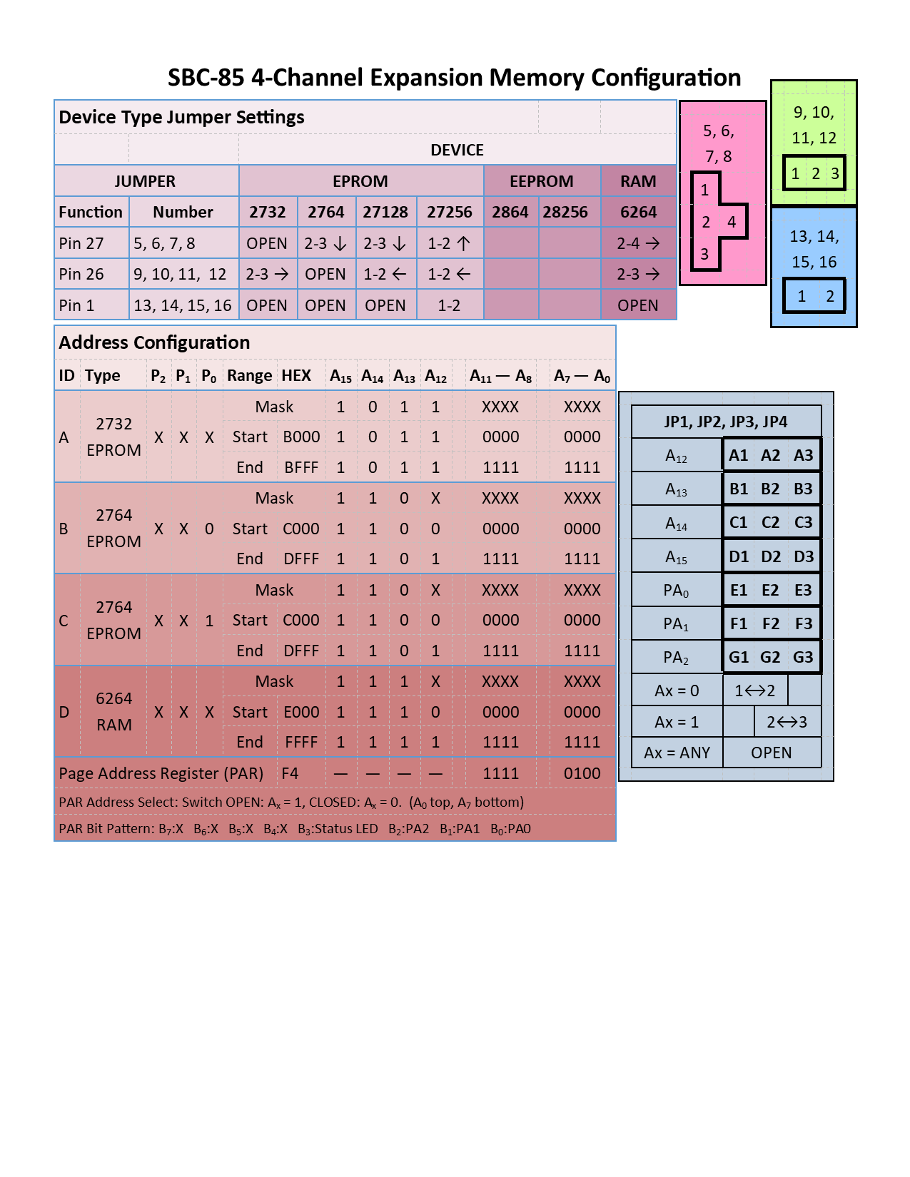
To solve the memory mapping problem and adapt to different chips of different size, each socket is given its own memory reservation option via jumpers. This does take a little more user understanding, but the SBC-85 seems to have brilliant users so I am not too worried about that. In practice, the user will set the base address being careful, as with any memory board, to make sure that none of the address selections overlap. To accommodate the various address block length for each chip, rather than just a “match address =0” or “match address =1” the user has three choices for the jumpers on address lines A15 to A12: address = 0, address = 1, or address = don’t care.
For example– If the user wants to install a 2732 at address 0x8000. Since this is a 2732 which is 4KB, the memory block will go from 0x8000 to 0x8FFF so the user will select A15=1, A14=0, A13=0, A12=0. If the next chip is also a 2732 and the user wants contiguous memory the next 2732 will have the jumpers set to 0x9000, i.e., A15=1, A14=0, A13=0, A12=1 and so forth. This example is the simplest because the EPROM takes all the space between the address options, i.e., setting A15-A12 alone claims the necessary address space.
However, when a larger chip is used, the least of the four address bits needs to be set to “don’t care” in order to claim sufficient address space. If the user wants to use a pair of 16kB 27128s, just looking at the number of address lines on the chip (A0->A13 = 14) tells us we can only use A15 and A14 to select the chip because A13 and A12 are part of the chip’s memory block. So for the first 27128 at 0x8000 the jumpers will be set to A15=1, A14=0, A13=don’t care, A12=don’t care. The next 27128 up would be set for 0xC000 A15=1, A14=1, A13 & A12 = Don’t Care again. While relatively simple the trade off is, of course, that the larger chips must start on an even boundary of their block size.
This addressing scheme essentially breaks the memory board down into four separately located memory blocks of the appropriate size for the selected chip. In the end, with a little bit of planning one or more of these boards can be a contiguous block, so no need to reassemble or recompile around memory gaps.
Finally, since the board obviously exceeds the addressable address space, there are three additional selection bits PA0, PA1, and PA2 which can be defined. The board has a 3-bit I/O port select register to set these three page address bits to turn the selected devices on or off. For example, if the user has selected 000 for these three using the jumpers, then that device is only enabled when the user has cleared those three bits in the board’s select register via an OUT instruction. Using the ‘Don’t Care” bits, allows any of the four memory devices to span more than one selection, i.e., a board with PA2=1, PA1=1 and PA0=”Don’t Care” will be enabled when either 110 or 111 is sent to the board select register. Setting all the jumpers to “Don’t Care” essentially removes this feature so there is one less thing to worry about.
 Craig
Craig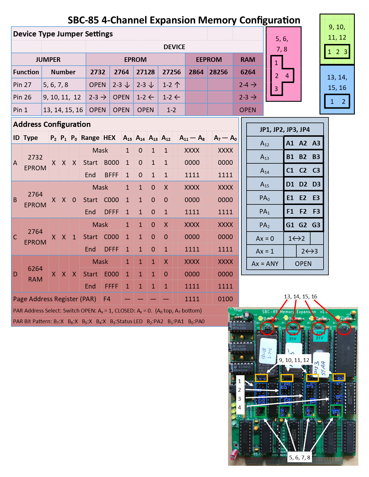
 SHAOS
SHAOS
 Keith
Keith
 Bentendo64