This is a very simple DIY design, you may cost within 2 dollars to get it.
Step 1: Early-stage Preparations
1 PCB Design Tool: EasyEDA
2 PCB Sample & PCB Assembly: JLCPCB
3 Components: LCSC
Step 2: Why I Start This Project
1 When we use ESP8266, there will be some program problems here.If you choose the ESP8266 with CH340, then the extra cost will be charged but many functions not needed for many projects.
2 If you choose to program it before welding,the line crossing is needed or you can reserve the recording interface, but these two ways also not that convenient and may take much space of PCB.
Step 3: Features
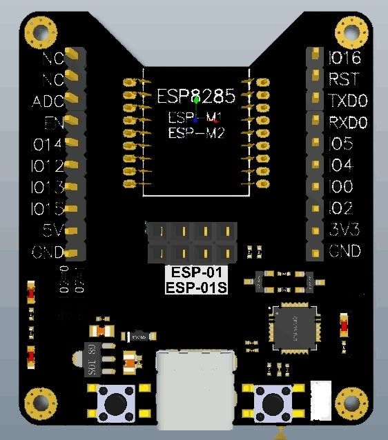
1 The project core around the CH340C chip, using serial port flow control and audion to achieve the 8266 firmware of a key burning, no need to plug the boot jump pin, very convenient.
2 The burning interface on the top and the following support two categories of packaging, pay attention not to confuse, the burning interface on the top of the use of a 90 degree bent needle, after the purchase of manual bending into 45 degrees, on the back of the needle is facing the board on both sides, do not weld backward.
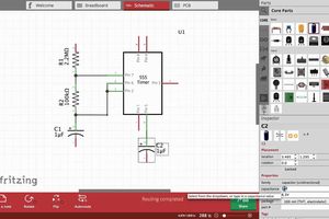
Step 4: Schematic

I use the EasyEDA to design this board, and it can generate the Gerber file and order on JLCPCB directly, quite convenient for us.
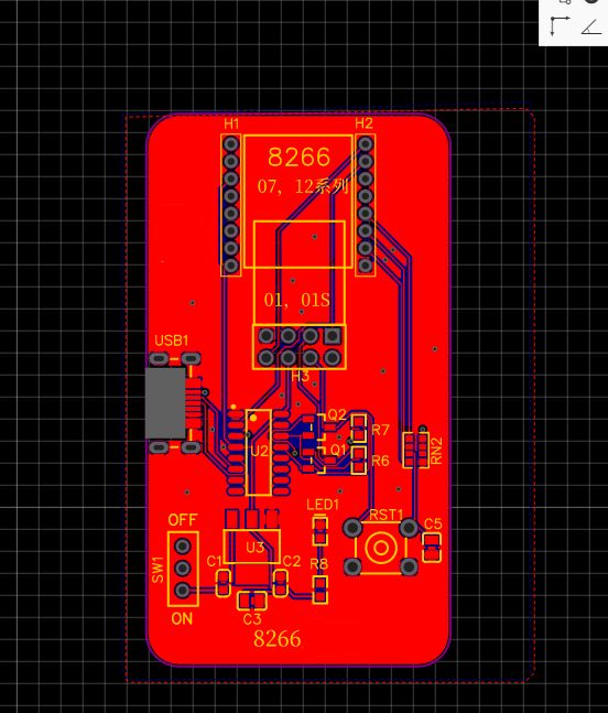
Step 5: PCB Files
 DIY GUY Chris
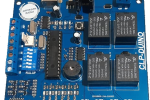
 Jefferson Bueno