I described in a previous post how you can write "assembly" for the TOM-1. This is the current way in which you'd write a program that subtracts two numbers on the data stack, and loops if the value is 0:
[start] -1 nand 1 add add branch0[start]
After the first label [start], every token in this program represents a single opcode that is executed every two clock cycles. There are a lot of examples of opcodes that manage the stack: dup, drop, load, store, and literal numbers like -1 all move data either from RAM or ROM or move data around the stack itself. But there's only two ALU operations: add and nand.
Writing loops using just two math functions is tricky. And while I'd love to build a high-level stack-based language just for this CPU, I wondered if there was a quick and dirty hack that I could procrastinate on first. Maybe that's getting the CPU to run C?
There is precedent for many homebrew CPUs to implement their own C-like compilers, common enough that CPU designs like the #Kobold K2 - RISC TTL Computer have pitched JSON standards for C parsing and lexing that would make adapting a C compiler to a new interface much simpler. Can TOM-1 run a higher-level language like C? Because TOM-1 is arithmetically underpowered, we really need to leverage an optimizing compiler or the C code we generate will be exhaustingly slow. Luckily, there are optimizing compilers for very simple CPUs, and there's precedent for directly emulating the instruction set of other CPUs as the #Gigatron TTL microcomputer does with its v6502 core or the #Novasaur Retrocomputer's support for the Intel 8080.
In the next few updates I'll evaluate Arduino (AVR) bytecode, then 6502 bytecode, and finally settle on a tiny processor I'd never heard of before(!).
I uploaded to Github the Digital circuit I've been using to simulate the TOM-1 in most of this project log. This implements the whole CPU and simulates the 7400-series chips a real version would use. In the later posts I'll start using a Python simulator written just for these experiments.
I'm thrilled to finally be able to demo a working program! Click the GIF above for higher quality.
This is a demo of TOM-1 loading the value 0x01 into the TOS (top of stack) Register, then adding TOS to itself every other clock cycle to produce a marching LED sequence (lower left, as well as the alphanumeric display). We are only cycling through the high 8 bits in this program for this demo, but TOS is two bytes wide and can support cycling through 16 bits.
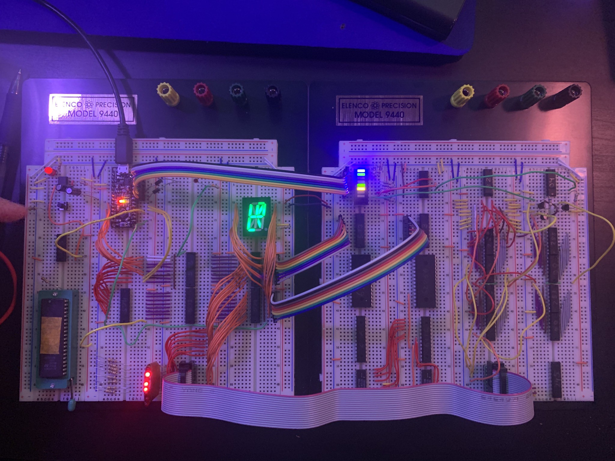
The most complex task has been building out the ALU. It's a 16-bit bus, and because the pin layout on the 74LS283 (4-bit add with fast carry) and 74LS00 (quad NAND gates) are staggered, wire placement took a lot of consideration. The chips are fairly crammed in on the rightmost circuitboards, so this took a few stages of wiring: first pairing each chip's inputs and outputs together (purple/grey wires), then wiring connections 4 bits at a time to the TOS Register, the Memory Bus, and the 16-bit output (yellow/red/orange); then wiring the TOS Register and Memory Bus lines to the 74LS573 latches where the ribbon cables from the left side are connected (green wires). This goes on to latch to a 16-bit value that can be loaded from ROM.
While it's referred to as a Memory Bus, none of the memory is actually hooked up yet: the 62256 RAM chips and the 6116 Stack chips aren't connected yet. TOS has a latch to copy its value onto the Memory Bus, normally so that we can load the TOS register into memory, but in this case we turn it on to let us add TOS to itself (like an assembly-level "double" opcode). Since there's only one real CPU register, there's not much to do until the stack is connected. But I'm thrilled to finally run blinkenlights :)
Source code of the program [4 bytes per opcode]: 0x02 0x00 0x00 0x01 0x00 0x00 0x03 0x00 ... (last four bytes repeat eight times, then Arduino resets)
Another in-progress photo. Here you can see a 16-bit value being loaded from “ROM” (which is substituted with an Arduino for now) into the Top-of-Stack (TOS) register. The TOS register is connected to the green 16-segment LED display on this breadboard. There are three reasons for including this display:
The first benefit of this display is that it gives a super easy way of referencing what value the TOS register currently has.
The second benefit is that by loading specific values into TOS, you can make the alphanumeric display show a single character at a time, for example, stepping through the letters “hello world”. Unlike ASCII, where letters are encoded sequentially, the values that correspond to each letter on this 16-segment display depend on how you wire the component. Unlike ASCII, this character encoding is entirely specific to this circuit. Instead I’ve taken to calling this character set it “TOMSCII” in the codebase 😉
The third benefit of this display is that the output pin of this component is essentially a 16-bit OR gate composed of DTL logic (diodes). This allows us to implement a JumpIf0 opcode: if the output of the display is 0V, this means none of the bits in the register are set. By boosting the output voltage we can use this as input to a flip flop that controls whether we jump or advance the program counter each clock cycle.
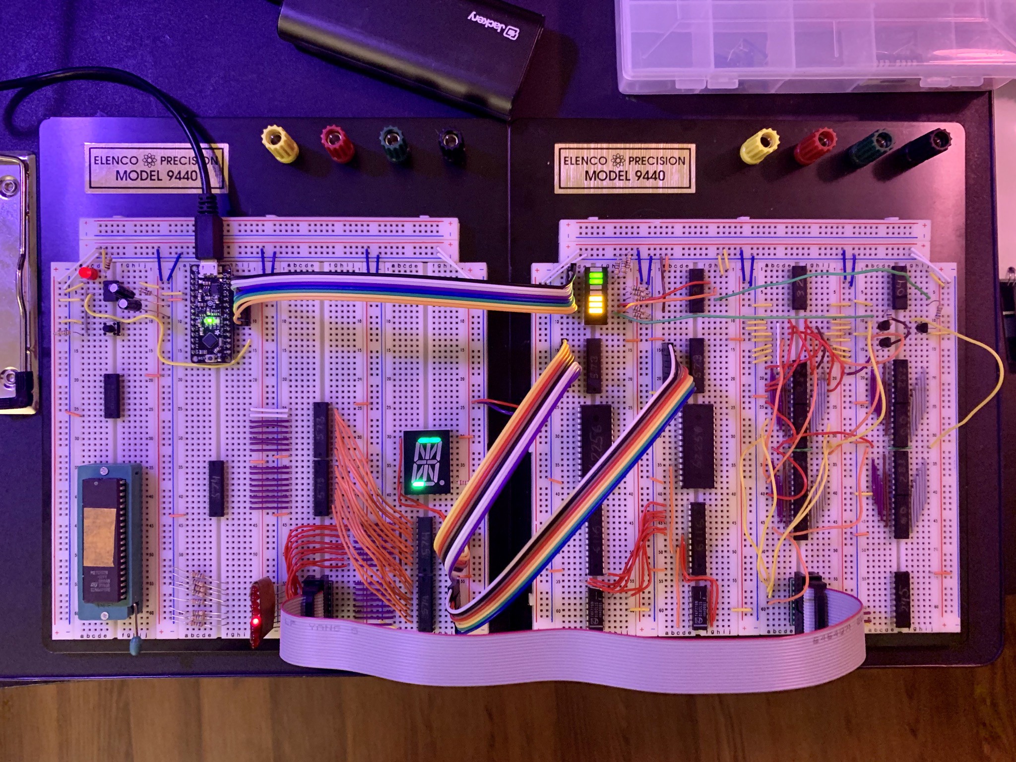
The TOM-1 can add two numbers together to get 0x10 (seen in the lower left red LED strip). The 16-pin grey ribbon cable connects to the ALU on the right (breadboards #7 and #8). I'm debating the best strategy to wire circuits together, going back and forth between ribbon cables and repositioning chips to allow better direct wiring.
When I started this project I wasn’t sure if I were going to attempt to breadboard this design, but now I’m grateful I tried. It looks like this will span several breadboards so I’ve connected two sets of four together, which should be enough? As a way of debugging the circuit immediately without fussing with EPROM programming and counter logic, I am using an Arduino-like from Adafruit to drive the ROM bus and perform branches. I also put together a step circuit using a 555 where each clock cycle can be controlled by a button press.
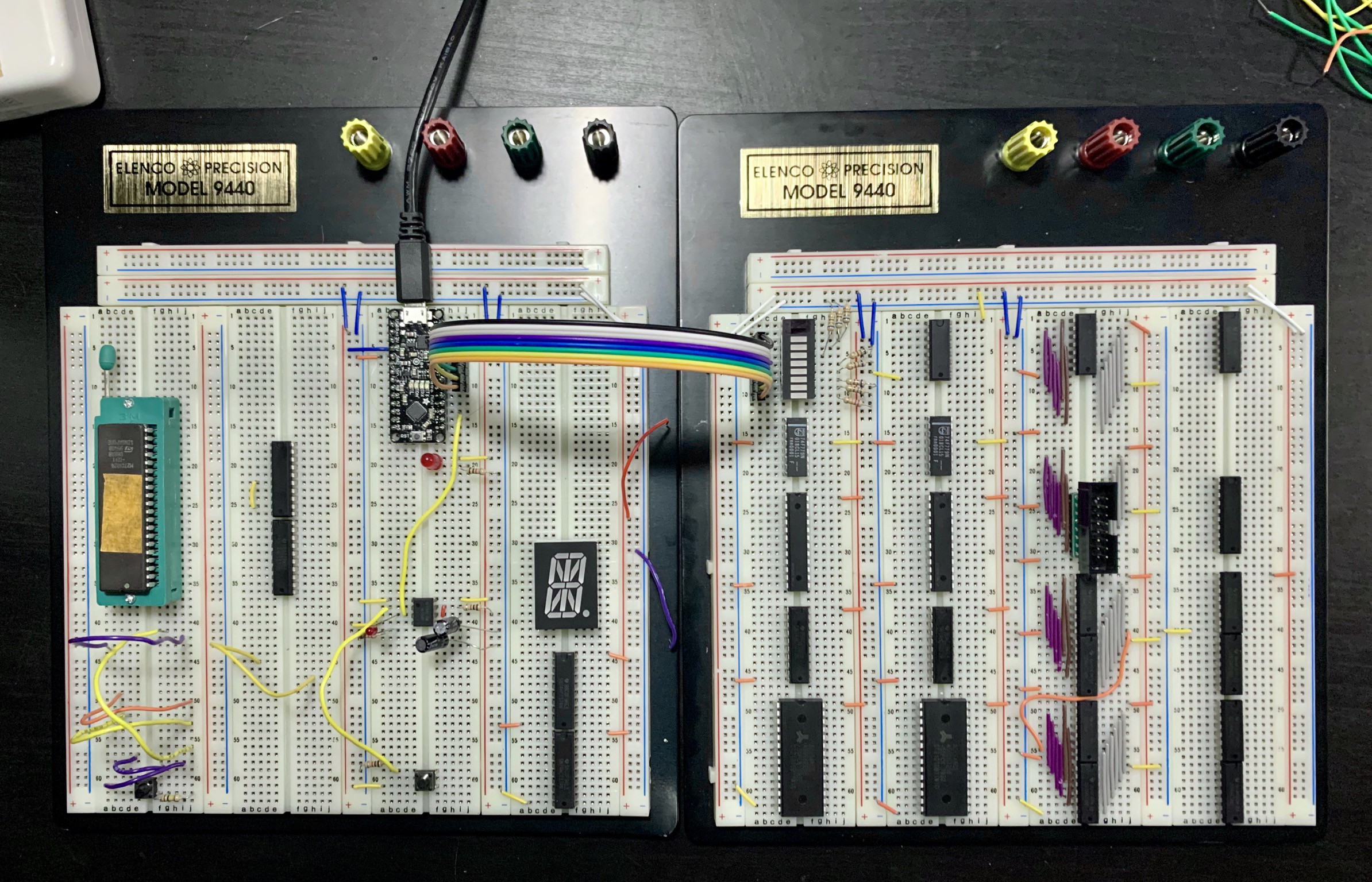
The biggest challenge seems to be how to wire up a 16-bit bus, which consumes a lot of wires and makes wiring really tedious. I’m trying to split all logic into 8-bit slices, so the high and low bytes of the CPU bus can be handled separately. On the right module, beardboards 1 and 3 correspond to the high byte, while 2 and 4 control the low byte. The 16-pin IDC interface is the TOS bus, which loops back to the input of the Top it Stack register on the left module. Hopefully this breakdown makes it easy to keep wires under control when I start putting together the bus.
My biggest blocker: I didn’t learn about the distinction between the 373 (silly pin order) and 573 (left to right pin order) before trying to use these chips. Now I’m stuck waiting for them to come in, since the alternative is cutting a lot more custom wire lengths!
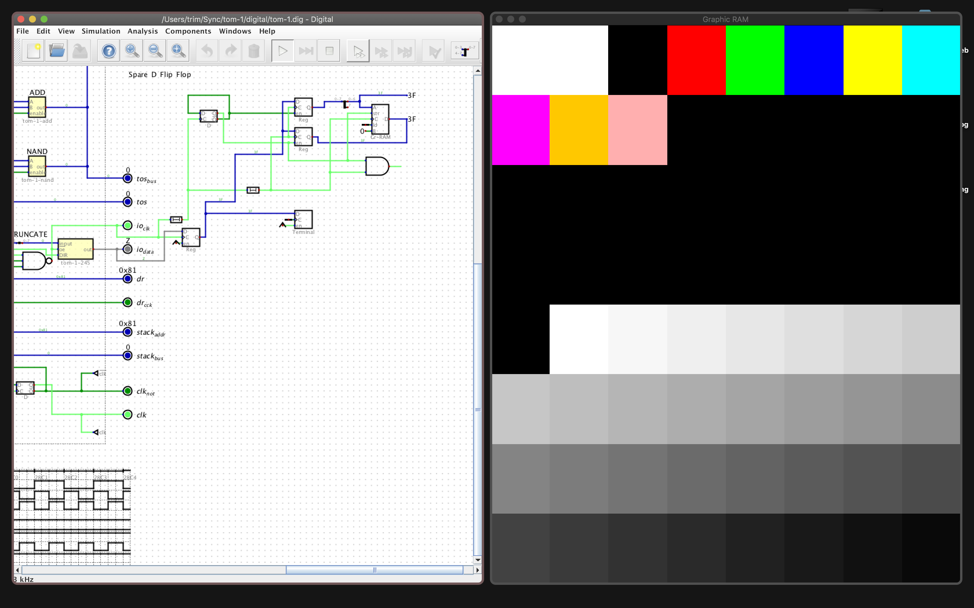
A short update: I figured out that Digital supports a fairly flexible Graphics integration called "Graphics RAM" that is a great way to test out CPU loops and timing, and also make demos more interesting. In the interest of keeping chip count small, I wanted to see if the TOM-1 could support just a single bidirectional transceiver (74LS245) for all of its I/O. I tested this out with Graphics RAM by first writing a byte for the address (into an 8x8 grid) and a second byte for the graphics value. With some additional circuitry, the TOM-1 can draw 256 color values onto a 8x8 Graphics display. The open question is whether it can do so using SPI to draw onto a command-based display, like Adafruit's SPI TFT display.
I finally have enough parts to start breadboarding! I bought a 3742-Contact Point Elenco Breadboard which houses four regular sized breadboards. I think I'll wind up needing two of them. Here's an animation of me testing out the 74LS283 adder chip, with inputs A1 and B1 being controlled by the buttons and Σ1 and Σ2 being wired to the LEDs. I've never done a massive breadboarding project like this before, so I anticipate being pretty slow at it.
Having done as much as I can for the moment in Digital, it's time to switch over to validating in circuity. I bought an EPROM programmer and UV eraser online for the M27C1024, a 256x16 bit EPROM that this is now obsolete, but which has the rare property of having a 16-bit wide data bus. Getting one of these EPROMs will probably take another week or two.
I needed a better way to test the branching logic of the CPU and decided to come up with a fairly basic "assembler". Taking inspiration from Forth, we can invent a very simple programming language from scratch taking a string, splitting all the whitespace into a set of tokens, and then converting each token into a 4-byte instruction in the code binary that the circuit uses to operate. With just a little compiler magic we can throw in some convenience features like named labels and mixed decimal and hex (0x-prefixed) numbers.
Here's an example of a test that verifies subtraction:
This language isn't actually Forth but something much less powerful. Here's the module "tom1" imported at the top of the file: tom1.py
So in the above script, call to generate("""..."""") will take a TOM-1 "script" as its first argument and actually compile it, generating a .hex binary file that can be used by the CPU in the simulator. This function generate() also returns a value labels that can be used to actually run the test. The methods debug() and the rest that follow generate() are actually Python code to interactively run the CPU, to step the CPU until we hit specific labels, and then validate if all the CPU values are correct. If the script doesn't throw during a call to validate(), then the test succeeded.
Let's look at the at the first and last lines of the script inside the triple quotation marks ("""):
"""
[start]

...

0 branch0 start
"""
[start] declares a label that we can conditionally jump to. When the compiler sees it, it will treat the token start everywhere else in the script as a reference to the location in the program where you wrote [start].
The token 0 means the CPU will push the number 0 to the stack with its "push_literal" opcode. The next token branch0 is implemented on the CPU as a "jump_if_0" opcode that rewrites the Program Counter with a new address if and only if the value on the top of the stack is equal to 0. So 0 branch0 is a two-opcode way to "always branch". All the tests end with a jump to the start of the program since there is no way to stop the CPU...
The middle line in the script is the actual test:
0x8372 0x35aa -1 ~& 1 + + [check_subtraction]
This is actually an executable program that subtracts two numbers! The CPU needs a lot of assistance from a compiler to abstract this away, because the CPU can do very little. For now I'm forced to write this out by hand. Let's break this down in steps:
0x8372 0x35aa => We push these two values onto the stack. The top of the stack is now 0x35aa.
-1 ~& => We push the value -1 and then NAND the top two values on the stack. The token for the NAND opcode is arbitrarily ~& so it looks similar to the other arithmetic function +. After this opcode, the top of the stack will be equal to "0x35aa nand 0xFFFF", which is 0xca55. This is actually a bit hack that inverts 0x35aa without needing a dedicated "invert" opcode.
1 + => We need to add 1 to the inverted number. There's a difference between inverting a number and turning it negative, and that difference is two's complement.
+ => We add the top two values on the stack, which are now the first number we pushed (0x8372) and the two's complement of the second (0x35aa). Adding them together performs subtraction, and we get our one result on the stack: 0x4dc8.
And there you have it, arithmetic subtraction on the TOM-1 implemented in a blazing, uh, 14 clock cycles. The final token in the script [check_subtraction] is used for testing but also is a helpful comment, since this code is very hard to follow. Eventually I'll have to stop working on an assembler and start working on an actual compiler, so -1 ~& 1 + + can be tucked away inside a function.
When coming up with requirements for TOM-1, I knew that the opcode space would be limited enough that the system would probably not require microcode, since I had seen Forth implementations which did not require many instructions. This meant I didn't tackle the question of how opcodes actually would be decoded until later. This organically built up into a collection of signals I could embed ad-hoc in a binary generated by Python:
This function would write out the TOM-1 "push literal" opcode, by writing the CPU flags for two clock cycles (a full opcode) and a 16-bit operand. Take a look at the TOM-1 system diagram, or read this explanation: On the first clock cycle, we ask for the ROM to be on the TOS (top of stack) bus, for the D register to increment, and for us to write the value of TOS to the data stack. On the second clock cycle, we just leave ROM on the TOS bus. At the end of the second cycle TOS latches the 16-bit new value from ROM.
Having written this out, it's clear that describing these flags isn't helpful in forming an "intuition" of what is happening in the CPU with each opcode. After struggling with different 2:4 and 3:8 decoder strategies, I actually came across another microcode-less design which seemed to share some design goals, as well as having an 8-bit opcode width. Here is the opcode format used by the #Microcode-less TTL CPU :
The instruction decoder is composed of two demultiplexer ICs (2 x 74HC138) and is driven by the instruction register. A CPU instruction word is 8 bits wide, 3 bits select the data source and 3 bits select the destination. Each demultiplexer ICs apply the control signals to the selected destination/source at the execute phase (3. phase). The instruction decoders (2x74HC138) use up 6 bits of an instruction word, I used the remaining two bits for instruction modifications [carry and zero].
Just from looking at this encoding, we can infer a few things about the CPU:
It can only move a value from a "src" register to a "dst" register each clock cycle
There are up to eight "src" registers and "dst" registers, and may be discrete sets
Conditional logic is done via the "on zero" flag
This is confirmed in the project's description which reads "Eventually each CPU instruction is a hardwired MOVE instruction, the instruction code itself determines the component that will be the data source (e.g. accumulator, input port, RAM, program memory, etc...) and the data destination (accumulator, adder, inverter, output port, program counter, etc...)." The circuit is an example of transport-triggered architecture. From taking a look at the schematics, "src" registers appear to include the accumulator and program memory, and destinations include the program counter, accumulator, adder, and inverter. Other chip enable lines appear to be cycle-dependent.
TOM-1 Opcode Design
We can look back at the TOM-1 system diagram. TOM-1 design and draw some parallels. While I wouldn't describe the architecture as TTA, it does have three "concerns" each clock cycle:
Selecting a stack register (D or R) and incrementing or decrementing it
Computing a new value to be loaded into TOS (the accumulator)
Performing a stack or ram load or write
With this in mind, here are the first 4 bits of the TOM-1 opcode which will probably not change:
DR_SEL — LO selects the D register, HI selects the R register.
DR_UP — LO decrements, HI increments. This flag does nothing if DR_CCK is LO.
DR_CCK - HI enables clocking (incrementing/decrementing the register) and LO disables it.
TOS_DISABLE — When LO, TOS output is enabled. This means that TOS will be available on the BUS as an ADD and NAND operand, as the RAM address input, and an input to a buffer connected to the stack bus. When HI, TOS is disabled.
These signals cover concern #1 and part of concern #2.
After reworking the rest of the signals, I came up with the following design, build around using dual 2:4 decoders. The next two bits select from one of four behaviors using the stack bus:
Stack outputs value to stack bus (as an operand)
TOS writes to stack
Stack writes value to to RAM
RAM writes to stack
The last two bits select from one of four behaviors on the TOS bus:
Enable buffer from ROM to TOS bus
NAND result is on bus
ADD result is on bus
JumpIf0 is performed
This covers the rest of the CPU's concerns. Though it doesn't impact the TOS bus, including our conditional Jump flag here makes sense–we perform a jump if the value in TOS is 0!
Putting this all together as a graph:
Opcode format for the TOM-1:
    7        6        5        4        3        2        1        0
+--------+--------+--------+--------+--------+--------+--------+--------+
| DR_SEL | DR_UP  | DR_CCK | TOS_EN |STACKb_1|STACKb_2| TOSb_1 | TOSb_2 |
+--------+--------+--------+--------+--------+--------+--------+--------+
Takeaways
A new opcode is read clock cycle, and it cleanly describes the behavior for that cycle of a) both of the stack address counters, b) whether TOS is an operand in ALU calculations, c) the behavior of the stack bus, and d) the behavior of the TOS bus, which is written to TOS on even cycles. I have to go back and clean up the old signals in my Python code, but this should make it easier to know for each opcode a) which part of the circuit is affected by each flag and b) for what reason.
Both small-ALU designs only required small decoders. It looks like the Microcode-less TTL CPU does not need two 3:8 demultiplexers and could also settle for 2:4, but the schematics may be out of date.
Because the TOM-1 is a stack machine, it has to dedicate a lot more control lines to register management. Aside from the program counter, the Microcode-less design has one register (the accumulator) but TOM-1 has three (TOS, D, and R).
Both designs use a decoder to select ALU instructions and another decoder to facilitate register transfers.
The Microcode-less TTL CPU has more room to expand opcodes, but the TOM-1 does not.
A note about expandability
On this last point: once I felt satisfied with the basic TOM-1 design, I went back to investigate how to add I/O to the system. It's fairly trivial to hook up a latch or a bidirectional latch to the TOS bus, and at first I thought about implementing a single 3:8 decoder to select all these different operations: ADD, NAND, IN, OUT, etc. But! Because this is a stack machine, there are some harsh tradeoffs to this design. If you are trying to stream data fast, it must come through TOS by popping off the stack. But the stack is limited to 256 bytes, which is partly consumed by program code already. Whereas RAM is plentiful if the CY62256 is used (32K values).
After rethinking the decoder design, I considered how a 2:4 decoder would work, and realized that the arbitrary TTL gates and ad-hoc wires I'd been using (e.g. "STACK_W_nR") might be more intuitive if they were just a decoding. However, 2:4 is a small number of options to decode to and it still limits what can be done with the RAM device connected to the stack bus. Taking the above encoding and adding onto that an "input" or "output" operation using the available bits seems unlikely. But! Every RAM write and read shares a common input value for its operation: its address. And the maximum address of the CY62256 is only 15 bits. So A16 might become the ninth decoder bit I need. 😂 Similarly, we might be able to implement HALT by jumping to an odd address.
 Tim Ryan
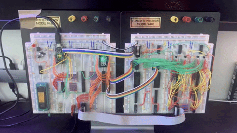

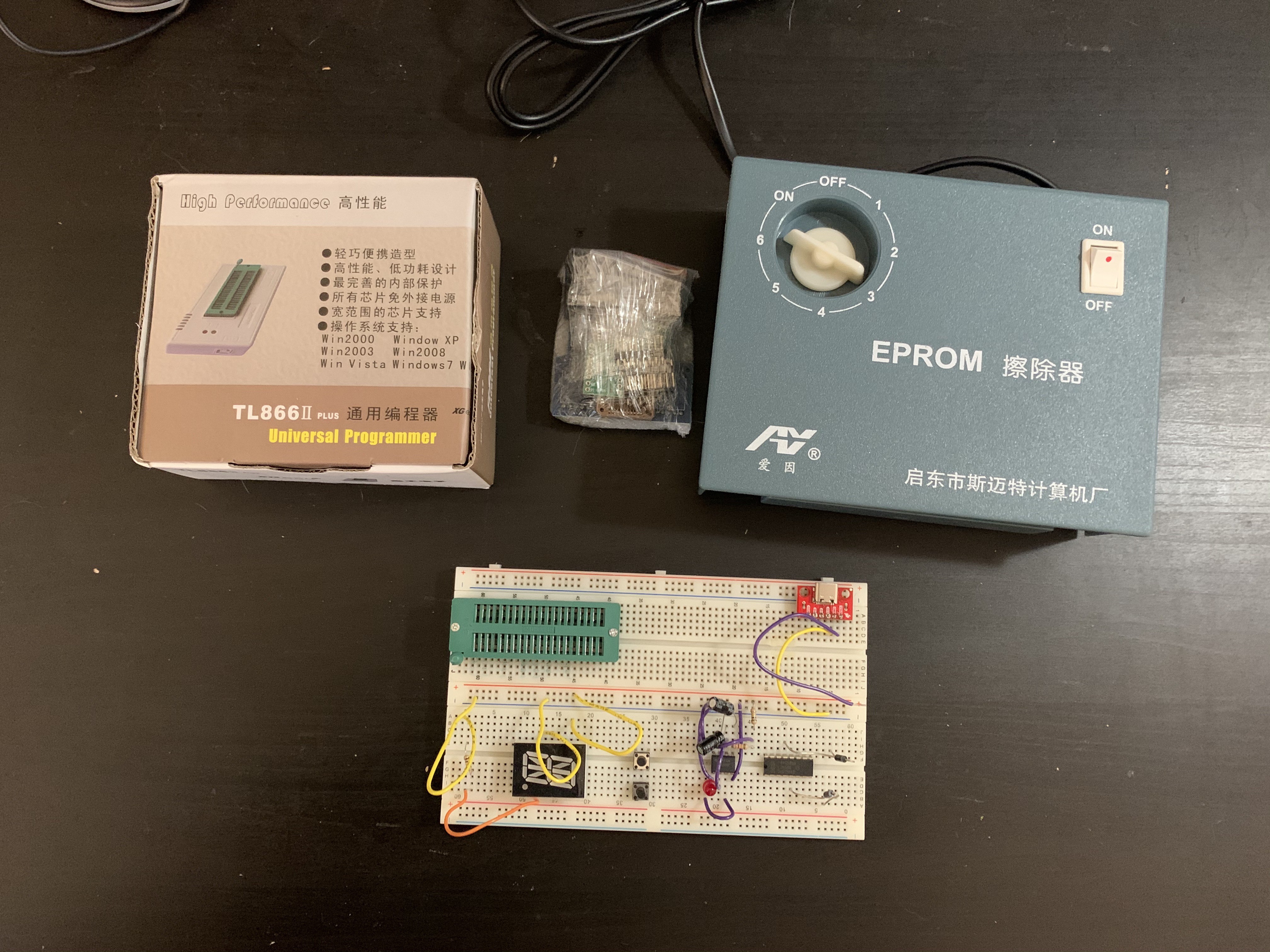 Having done as much as I can for the moment in Digital, it's time to switch over to validating in circuity. I bought an EPROM programmer and UV eraser online for the M27C1024, a 256x16 bit EPROM that this is now obsolete, but which has the rare property of having a 16-bit wide data bus. Getting one of these EPROMs will probably take another week or two.