To keep it short : life is life. Demanding baby. Lot of time spent on solving problems at my job. Too much tired to work on my projects. But at lest i solved nearly all of the stacked problems at my job and my little boy gave me some space.
So 6 weeks ago I FINALLY had free time and ENERGY to get back to my projects ! YES !
Being far from it for some time wasn't bad. When I looked at my notes (and after a lot of hours of looking at others videos / projects) it was clear. I missed/ignored one important information I read when starting this project.
The CPU !!!! The CPU have two PCMCIA bus to manage extensions. How could I've missed that ! I felt stupid, angry, overjoyed and on fire all at the same time...
After studding how the PCMCIA bus work, I understood more about the board and it's schematic. I had guesses some lines correctly, some other seemed strange, so more guess until it felt coherent. So more pins where identified.
There's a card detect signal. During previous my tests (didn't write them down in the buildlog) i found that pulling it down to GND with a 5K had an effect on the scope. It detected that a card was inserted but it was unable to detect it correctly. Now I know it's just on step to the card detection.
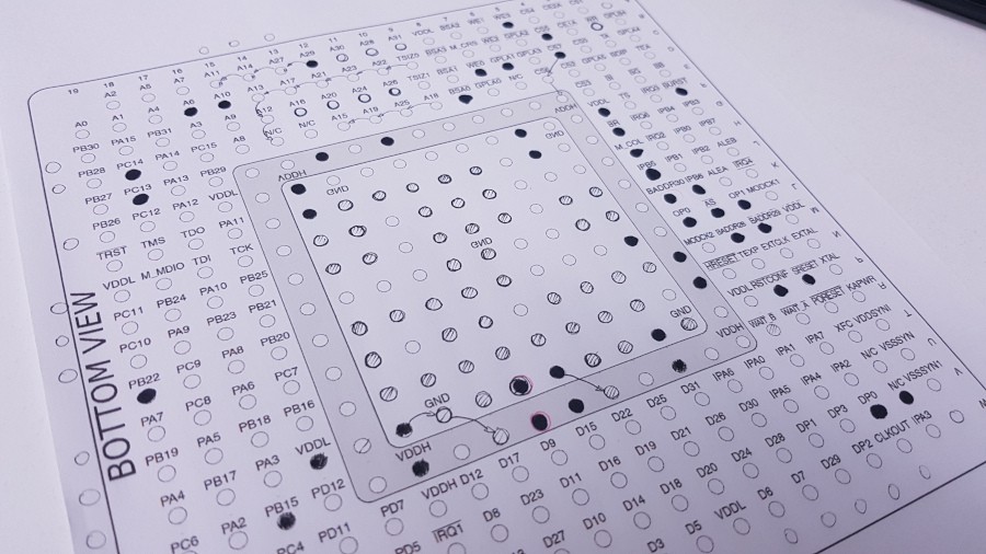
All of the data pins and data lines I identified previously left me with doubts. After reading the CPU documentation, I knew why. All the address pins are swapped. The CPU is BigEndian and the PCMCIA is LittleEndian. And more than that. the address lines for the PCMCIA is shifted by 6 bits. The CPU as 32 addrs lines, but only 26 for PCMCIA. CPU A32 is PCMCIA A0, and CPU A6 is PCMCIA A25.
Now I knew. I knew how the card was identified. One LCX245 act as a 8 bit ROM mask connected on the D0-D7 bus and selected using /CE2 and R/W signals from the PCMCIA bus.
But no LCX245 in my stock. Had to buy some.
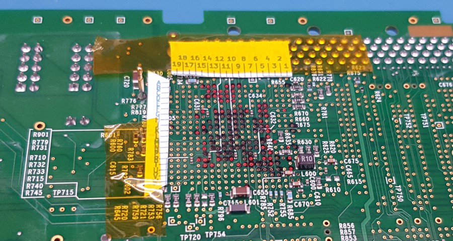
Waiting for them I got my 3032C, opened it, put the mother board out, more paper, more pen, made a tool to probe a large area on the mother board, and it was a stop. The vias under the BGA package are a mess. Not aligned with the pins, missing holes, .... cold shower. I already knew it, but I forgot.

After a good night of thinking instead of sleeping, I decided to do the inverse. Why not probing the vias with the pins i already know from the expansion port ?
After pocking around like that a pattern started to emerge on the vias. Some lines was just pushed left or right, other top or down and even in diagonals.
The CPU as a lot of GND pads, all in the center. A black sharpy, and all pins connected to GNDs was marked. A red sharpy, and all VDD pins marked.
Time to poke around more and get the exact position of each pad on a paper. Every pins identified is marked with the sharpy. It helped a lot and more pins were identified or corrected on the expansion slot. And like always, more paper ...

And then.... three weeks ago the TTLs arrived.
 PMercier
Discussions
Become a Hackaday.io Member
Create an account to leave a comment. Already have an account? Log In.