 Leonardo Ward
The following list presents some recommendations for future versions of the PCBs (Onboard Gateway V1.0, Buoy A V1.0 and Buoy B V1.0):
- Change the text that identifies the polarity of the terminal block DCin in the Onboard Gateway V1.0.

The problem is that the mount hole in the PCB identified (using white text) as "-" is connected con DCIN + in the USB LiIon/LiPoly charger. Also the mount hole identified as "+" is connected to the ground plane.
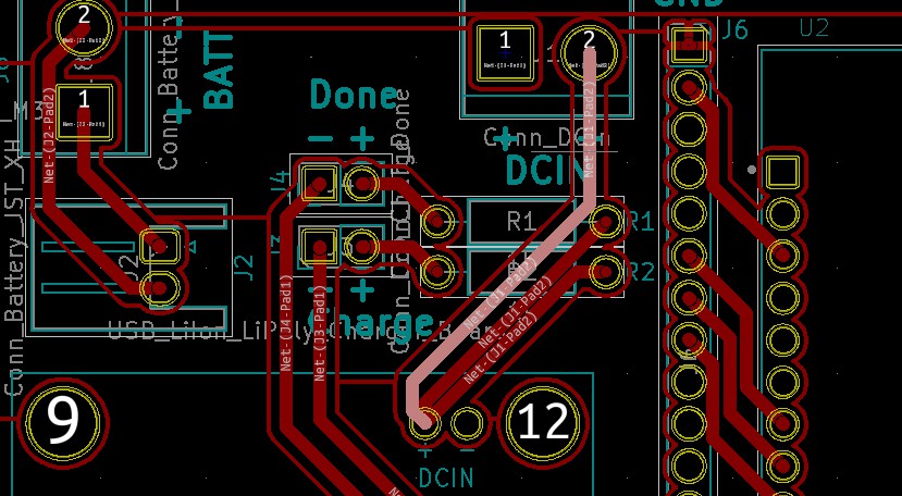
The "-" text should be changed to a "+". and the "+" text should be changed to a "-".
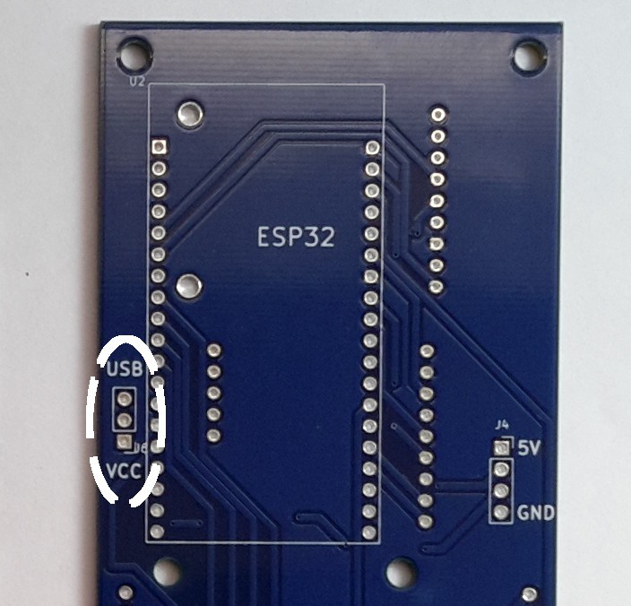
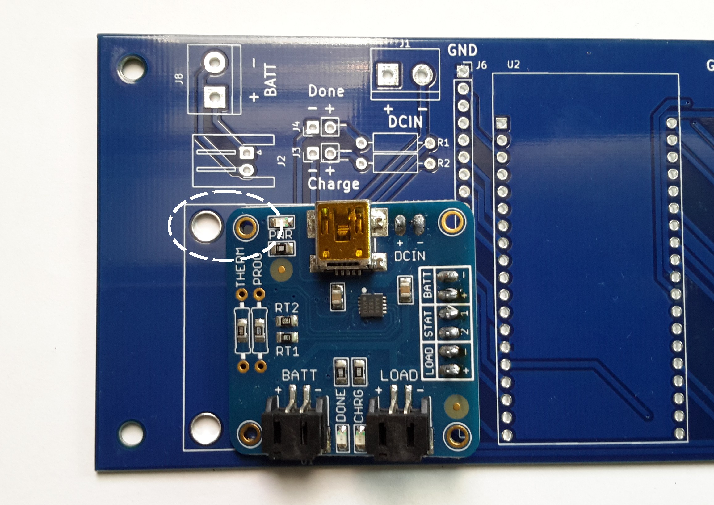
- Add text to identify VCC and USB in the J5 connector in the Onboard Gateway V1.0. This connector allows the user to select the power source for the ESP32 (VCC or USB).
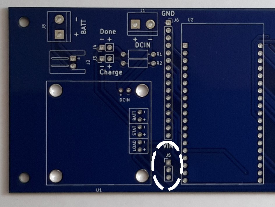
The J5 connector has 3 positions:
- Connected to Vin
- Connected to the EXT_5V pin in the ESP32.
- Not connected.
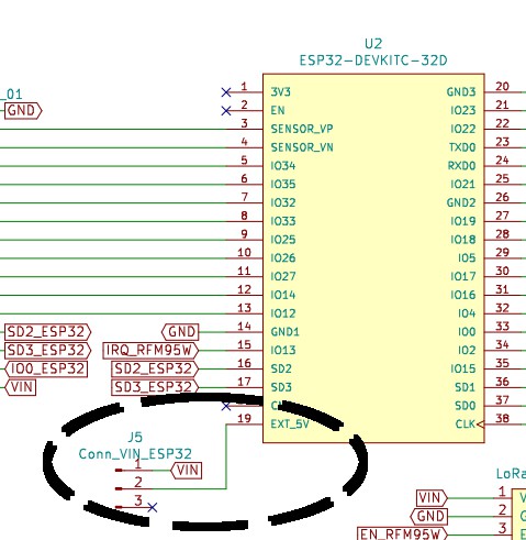
The objective of J5 is to solder a CONN HEADER VERT 3POS 2.54MM in the PCB and then use a CONN JUMPER SHORTING .100" GOLD to define the power source of the ESP32. If the jumper connects 1 and 2 then the ESP32 is connected to Vin, if the jumper connects to 2 and 3 then the ESP32 es not connected to Vin, in that situation the ESP32 can be powered through USB. Text should be added to this connector to identify the jumper alternatives, like the following image (Buoy A V1.0).
- When the switch is turned off in the Onboard Gateway design, it is not possible to charge the battery. The battery can only be charged when the switch is on.
- Add a capacitor to the VCC line in all the PCBs (Onboard Gateway V1.0, Buoy A V1.0 and Buoy B V1.0).
- Add a text describing the polarity for the JST-XH J2 connector in the Onboard Gateway V1.0.
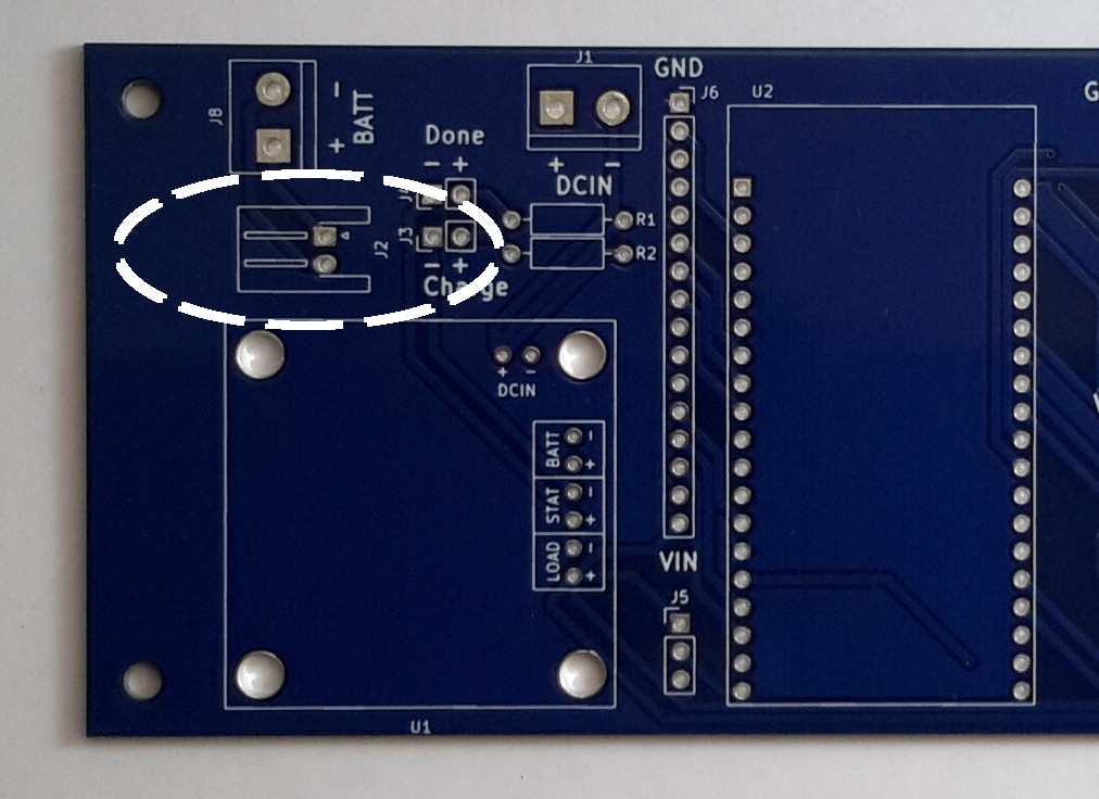
J2 can only be connected in one way, but adding text to the PCB can be helpful during debugging.
- Add the switch to the PCB design of the 3 boards (Onboard Gateway V1.0, Buoy A V1.0 and Buoy B V1.0). The JST-XH connector directly connects the battery to the design, so it is not possible to turn off the boards if you use that connector.
- The pin IO0 is connected to the label IO5 in Buoy B V1.0 and IO5 is connected to the label IO0. The board requires those labels to be renamed in the schematic. Those pins are connected to the J7 Conn_Extras connector that can be used to add more modules to the design.

- Augment the diameter of the mount holes in the PCB, difference in the precision and tolerance of the machines used to manufacture the PCBs can make the mount holes slightly smaller. In the current design, if the mount holes are slightly smaller, the header will not fit in the PCB.
- Adjust the size of the screw holes for the USB LiIon/LiPoly charger in the Onboard Gateway V1.0.
- Add internal leds for the PCBs. The Onboard Gateway V1.0 has connectors for external leds (male headers), but the design can also benefit from having internal ones (directly soldered). Buoy A V1.0 and Buoy B V1.0 have connector with the extra pins available in the ESP32-DEVKITC-32D, so it is possible to connect leds to the design, but those boards can also benefit from having internal leds (directly soldered).
Discussions
Become a Hackaday.io Member
Create an account to leave a comment. Already have an account? Log In.