PCB
Today the PCB has arrived. So tomorrow I will round up he chips and start the assembly. Flash the chips and with some luck it will fire up.
The most important thing to check here is if rst7.5 is trouble free from other programs hijacking the interrupt.
Next Version
Yes, I am thinking of that. But I have to check that the current design works first. The idea is baby steps, make debugging much easier.
The current version has 32kb RAM and 32kb of exposed ROM (i.e. Flash). It uses A15 to control the boot-up logic.
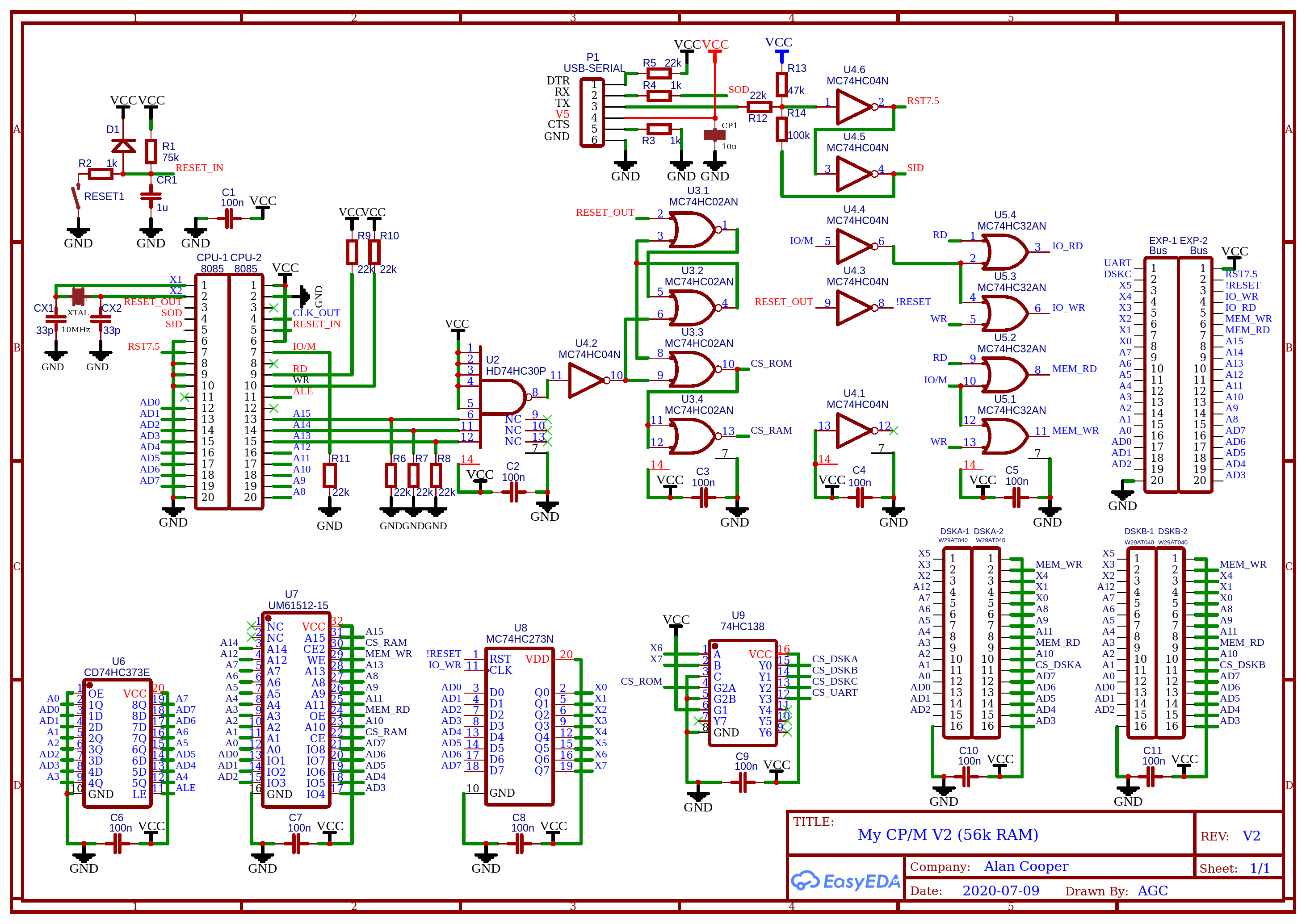
I can increase the RAM by reducing the exposed ROM, by using (say) A15, A14 and A13. This will give me 56kb RAM and 8kb exposed ROM (i.e. the full boot, ccp, bdos and cdos code). Now, I could increase the RAM further but this configuration work well with the 29AT040-90B Flash chip. The configuration give me 4x Flash disks of 512kb and 56k RAM. Here is the new schematic:

Instead of using a fourth Flash disk, the slot could be used for an UART and other hardware.
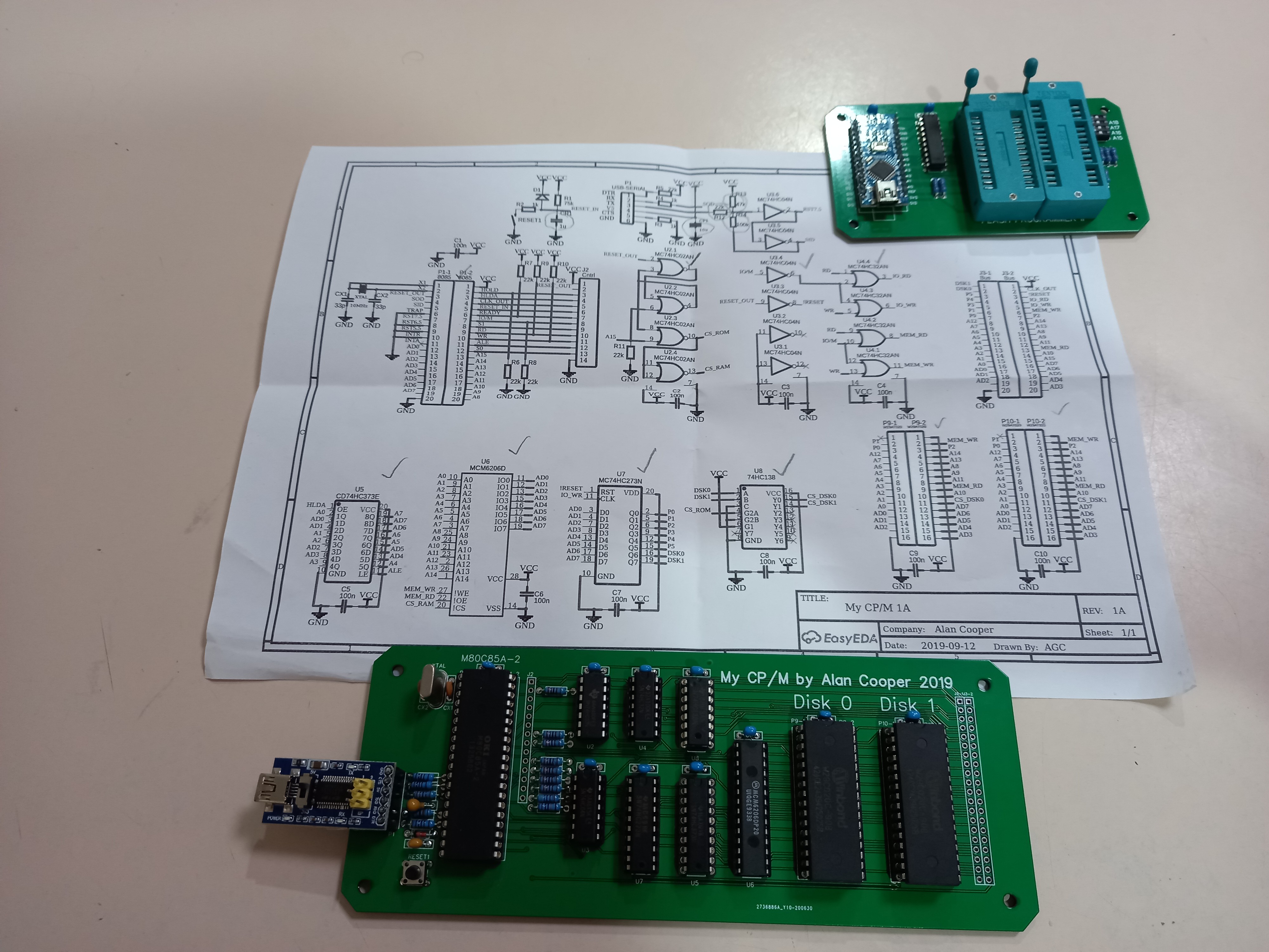
Assembled CP/M V1A this morning:

Next is to format the Flash Chips and load the system files.
Z80 Interrupts
I looked at the Z80 interrupts and found the "Mode 1" must be what most other CP/M systems must be using. It functionally equivalent to RST7.5 on the 8085 but the address is 0038h rather than 003Ch.
AlanX
 agp.cooper
Discussions
Become a Hackaday.io Member
Create an account to leave a comment. Already have an account? Log In.