In theory, there is nothing complicated about multimeter, as usually up to the point of meeting the reality.
The main part of multimeter is ADC, converting voltage to digital value, to be processed and displayed. Well, ADC directly measures voltage, that goes for the voltmeter part. For measurement outside the ADC input range, voltage divider (allowing higher voltage to be measured) or amplifier (for lower voltages) is required.
To measure current, usual method is to convert current to voltage. Fortunately, there is very common part converting current to voltage - a resistor. In order to have the option of changing measurement ranges, resistor switching is usually applied.
To measure resistance, one needs current source to push current through the unknown resistor, while the voltmeter part of multimeter takes care of measurement of voltage drop on the resistor, being proportional to the resistor value.
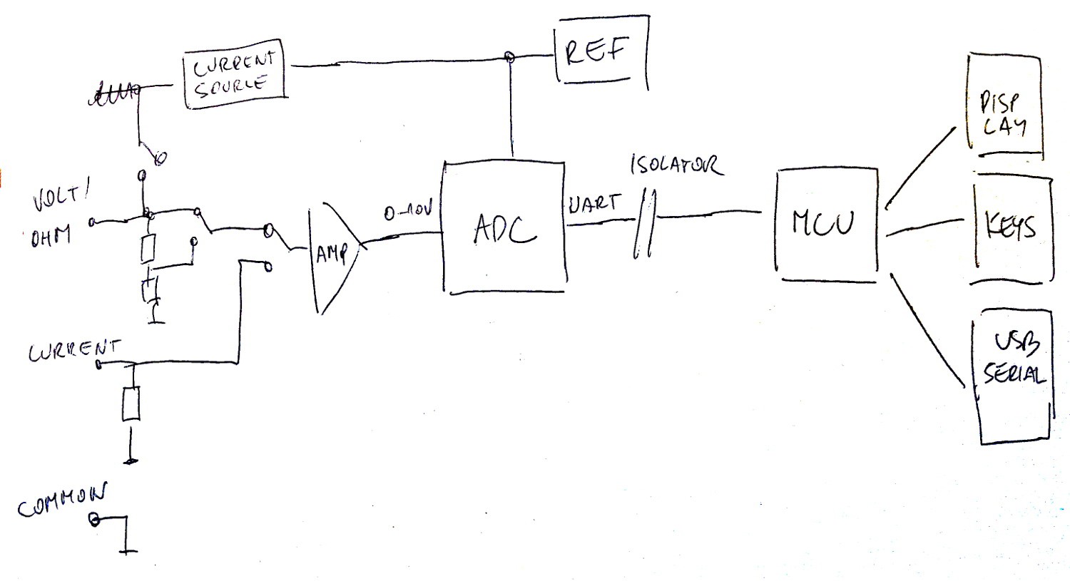
That is the simple part and really, majority of multimeters do operate in this way. I sketched a quick sketch of such as multimeter

As you can see, it's really that simple, but this picture already uncovers a few usual devils hidden in details.
First of them is voltage reference above the central, ADC part. This voltage reference should be as stable as possible, with regard to temperature and ageing. It doesn't need to be very accurate (non-accurate voltage can be "calibrated out") but drift with temperature and age is hard to predict and compensate for.
Another part that makes the design a bit more tricky is isolator. Since the measured voltage could be on any potential, perhaps floating on higher voltage or you may have two multimeters measuring at different part of the circuit, it is usually needed to have the COMMON (black wire of your typical multimeter) disconnected from power ground or each other. That's why the reference/amplifier/ADC part is usually "floating" or "guarded" (often referred as inguard part) and the MCU/interface/user IO is usually "grounded", via power outlet or USB or other connection to PC (usually referred as outguard part). This separation is usually not needed for handheld multimeters, operated from battery, being floating per design.
ADC
The main course of this project is ADC. While there are relatively good ADC in integrated form (AD7177, LTC2380), I opted for traditional multi-slope implementation, being used for decades in many high-resolution meter and still unsurpassed by integrated ADCs in electrical parameters. What more, this type of ADC is literally built from opamps and analog switches. I think it's very demonstrative how gigh-performance analo to digital converter can be built from a few vbasic building blocks, without the need for "black boxes".
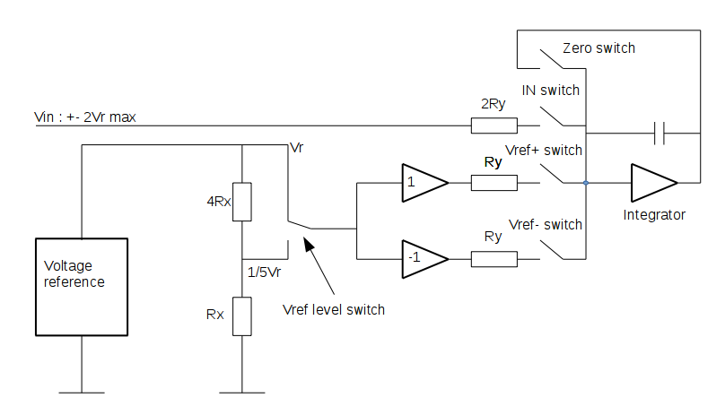
In some multislope ADC (by the way, reading this HP journal is very advisable for understanding how integrating ADCs do work) implementations, the integrator has numerous of switching sources - either input voltage, ground or Vref+/Vref- inputs via one or more resistors. This typically leads to composite custom resistor network, where most of the precision of the ADC is hidden. This is viable way for mass production, but not that much for one-off hobby prototype. Resistor networks with good tracking like LT5400 are available, with four resistors per package. In my original concept I'd need five resistors - one for input current integration, two for fast runup integration and two for slow rundown integration. Aside from resistors, I needed to solve another important decision - integration switches. With five resistors I need six (five plus integrator reset) switches. That is unfortunate, because switches like DG211B have only four channels per package. I can add more IC packages, but it takes more PCB area (not that much of a problem), but what is worse, requires longer tracks of sensitive signals and more convoluted guarding etc...
I solved this 6-switches problem by not having six switches: Unlike usual situation with four runup/rundows resistors feeding different integration currents from single Vref+/Vref- level, I opted for only two resistors and two different Vref+/Vref- levels.

This way I divided the problems into two smaller ones: Three resistors network with good tracking at integrator (marked as Ry resistors) input and another two resistors network with good matching in the Vref divider (marked as Rx resistors). Those two networks doesn't need to have good tracking to each other, however. There is third resistor network in Vref invertor. After Vref switch actions I leave quite bit of time for switched voltage to settle down and it doesn't seem to produce problems.

I opted for polystyrene capacitor into integrator, after I built dedicated tool to somehow compare dielectric absorption in capacitors and also because I stocked plenty of them. Since the integration frequency is relatively high, it's possible that other types would be OK into this application, I left this as exercise for later.
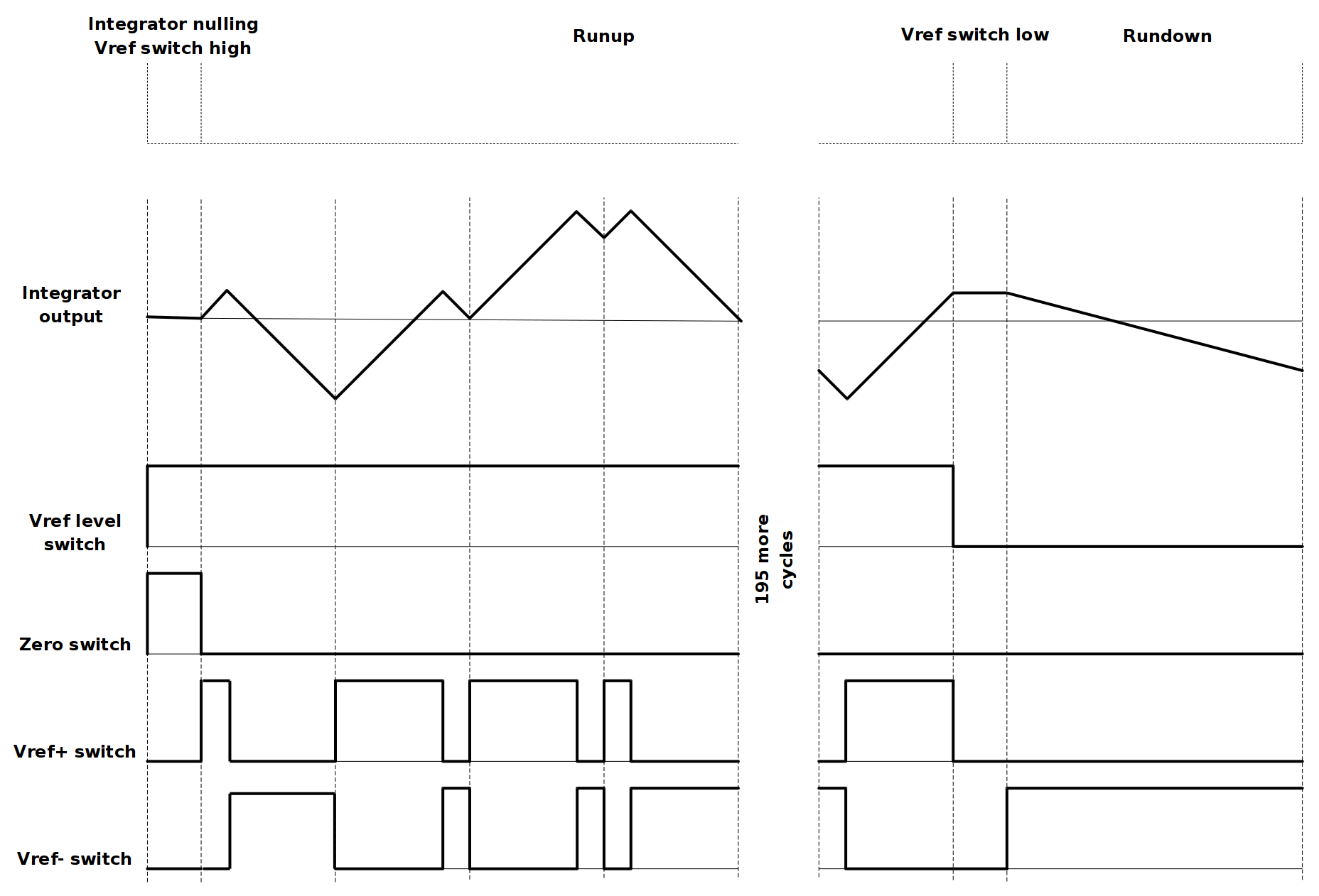
For runup I implemented simple algorithm to exercise both Vref+ and Vref- switches once per cycle, in effort to decrease charge injection nonlinearity errors (see diagram above).
Onboard reference is good old LM399AH. I employed FPGA for timing and control of ADC. I never really did any major project in Verilog and this was one of my first ones. First protoboard versions of my integrating ADC used MCU for timing and calculations, but I believed using FPGA is the right way to go, so it was strong reason (excuse?) to dig into Verilog more seriously than modifying simple blink-a-LED.
 jaromir.sukuba
Discussions
Become a Hackaday.io Member
Create an account to leave a comment. Already have an account? Log In.