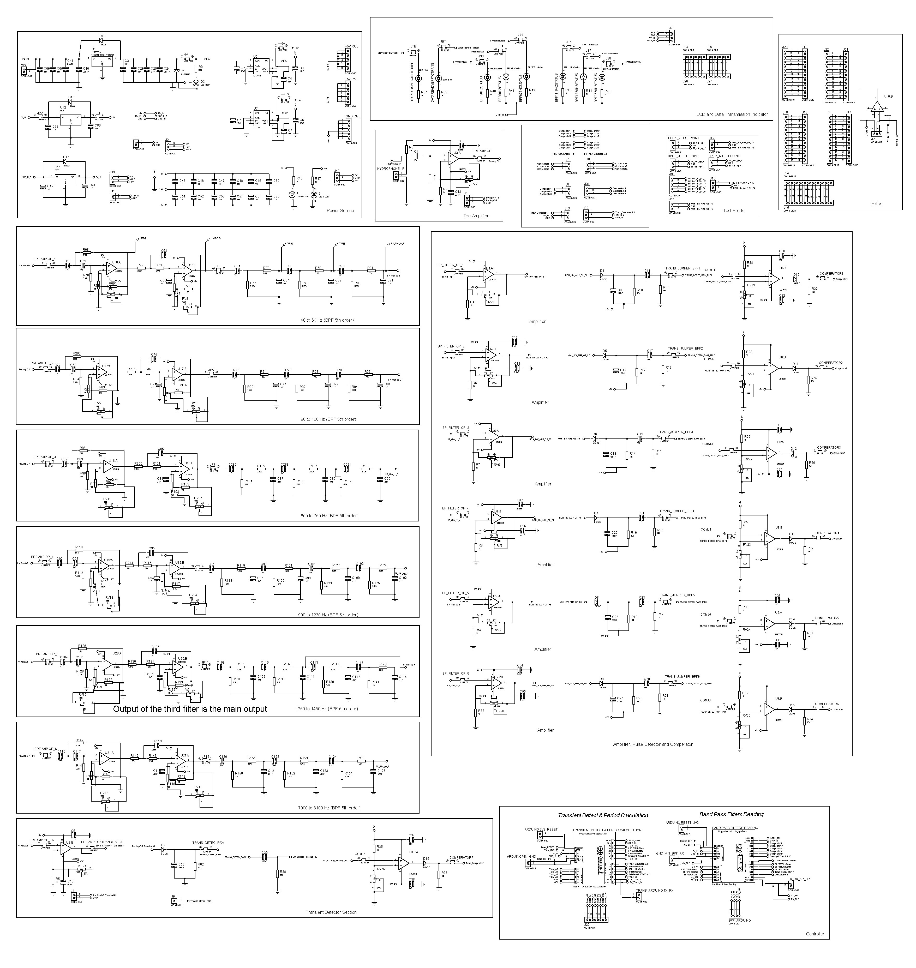
To minimize the size of the design a new schematic was prepared to combine the MotherBoard and DaughterBoard but it still have not been produced because later on the Buffer section of the design was needed to be added and also for the final design, the prototyping features are also needed to be removed form the PCB. But this can be used to create the BOM of the current design (MotherBoard and DaughterBoard).

 ifthekhar ahammad
Discussions
Become a Hackaday.io Member
Create an account to leave a comment. Already have an account? Log In.