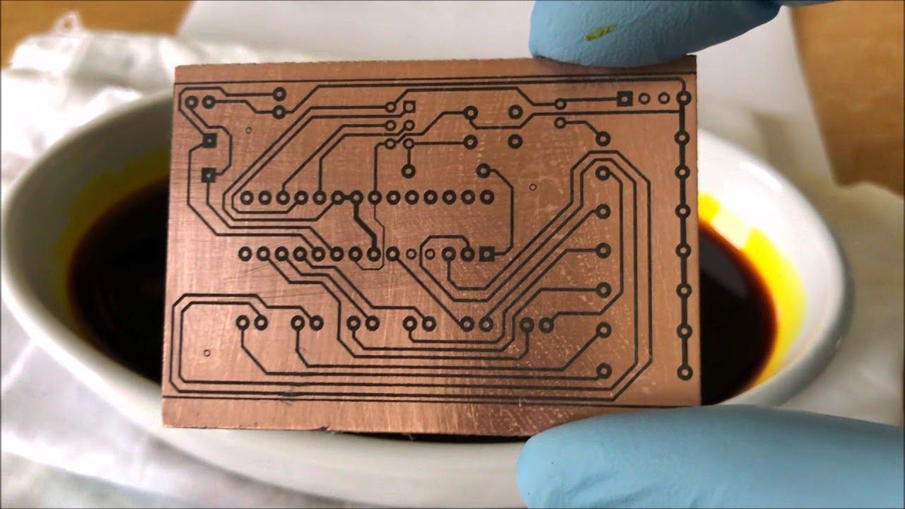
But lots of electronic hobbyists are interested in how to DIY PCB Board at home, so I would like to introduce 5 ways to DIY PCB at home.
Method 1 :
1. Make a board drawing. The soldering plate in the figure is represented by points, and the line can be connected by a single line, but the position and size should be accurate.
2. Cut and clean the copper foil surface according to the size of the board drawing.
3. Copy the drawing to the board with carbon paper. If the circuit is simple and the producer has some experience in board making, this step can be omitted.
4. Paste standard precut symbols with different inside and outside diameters (welding plate) according to the actual conditions of components; Then according to the current, paste different width of the tape line. For standard pre-cut symbols and tape, available at electronics stores. Common specifications of pre-cut symbols are D373 (0D-2.79, ID-0.79), D266 (0D-2.00, ID-0.80), D237 (OD 3.50, ID-1.50), etc. It is best to buy paper-based materials (black), plastic base (red) materials should not be used as much as possible. The common specifications of adhesive tapes are 0.3, 0.9, 1.8, 2.3, 3.7, and so on. The units are in millimeters.
5. Use a small soft hammer, such as smooth rubber, plastic, etc., to hit the drawing paste, so that it fully adheres to the copper foil. Key percussion line at the bend, joint. When the day is cold, it is better to make the surface warm with the heater to strengthen the adhesion effect.
6. Etching in ferric chloride, but it should be noted that the liquid temperature is not higher than 40 degrees. Then the metallic corrosion products should be promptly removed and washed clean, especially in the case of fine lines.
7. Make holes, make bright copper foil with fine sandpaper, coat with a rosin alcohol solution, and let dry until finished. The quality of this printed board is very close to that of a regular printed board. 0.3 mm tape can be passed between IC feet, which can greatly reduce the short jumper on the front of the board to save time and trouble.
Method 2
1. Print the circuit board drawing in the printer at the ratio of 1:1 on 80g copy paper.
Hand drawing is ok, but the base paper should be flat.
2. Find a fax machine, take out the fax paper in the machine and replace it with a hot plastic film (available in our company). Put the circuit diagram in the fax machine entrance and copy the circuit diagram on the hot melt film using the copy button of the fax machine. The "print manuscript" of the printed circuit board is then completed.
3, use double-sided tape to make a good picture of the plastic film flat on the copper plate. Pay attention to smooth, not wrinkle, tape can not cover the melted part, otherwise, affects the production of the circuit board.
4, with paintbrush paint evenly on the plastic film, pay attention to: not reciprocating brush, can only brush in one direction in turn, or plastic film together wrinkles, the lines on the copper plate will overlap. After the circuit diagram has been brushed, remove the plastic film carefully. Then a printed circuit board is printed. When left dry, it can corrode.
Method 3
1. Reasonably arrange the density and location of the components according to the shape of the components used in the circuit schematic diagram and the size of the printed board area.
The location of components should be determined in accordance with the principle of first large and then small, first whole, and then local so that adjacent components in the circuit are placed nearby and arranged neatly and evenly.
2. The connecting wire between the components shall not turn right angles at the corner and the intersection of the two lines shall use curve transition, shall not cross each other, and circuitous too far. If some wires really can't do this, consider printing wires on the backside of the board and connecting them to the front circuit with a pin, or alternatively using insulated wires when welding components.
3. It is better to keep the input and output parts far apart so as not to interfere with each other.
Method 4
Stick the post-it note to the copper foil coated with copper plate, and then draw the circuit on the veneer, and then use a knife to cut through the veneer layer, forming the required circuit, remove the non-circuit part finally with ferric chloride corrosion or current electrolysis method can produce a more ideal circuit board.
Corrosion temperature can be around 55℃, the corrosion rate is faster. Rinse the corroded circuit board with clean water, remove the post-it notes from the circuit, punch holes, and wipe clean the rosin alcohol solution for use.
Method 5
1. Cut the copper-coated sheet to the required size of the circuit diagram.
2. Put the wax paper on the steel plate, and carve the circuit diagram on the wax paper by 1:1 with a pen. Then cut the circuit diagram on the wax paper according to the size of the circuit board, and put the cut wax paper on the printed copper plate. Take a small amount of paint and talcum powder mixed into thin and thick suitable printing material, dip in with a brush to take printing material, evenly spread on wax paper, repeated several times, printing board can be printed on the circuit.