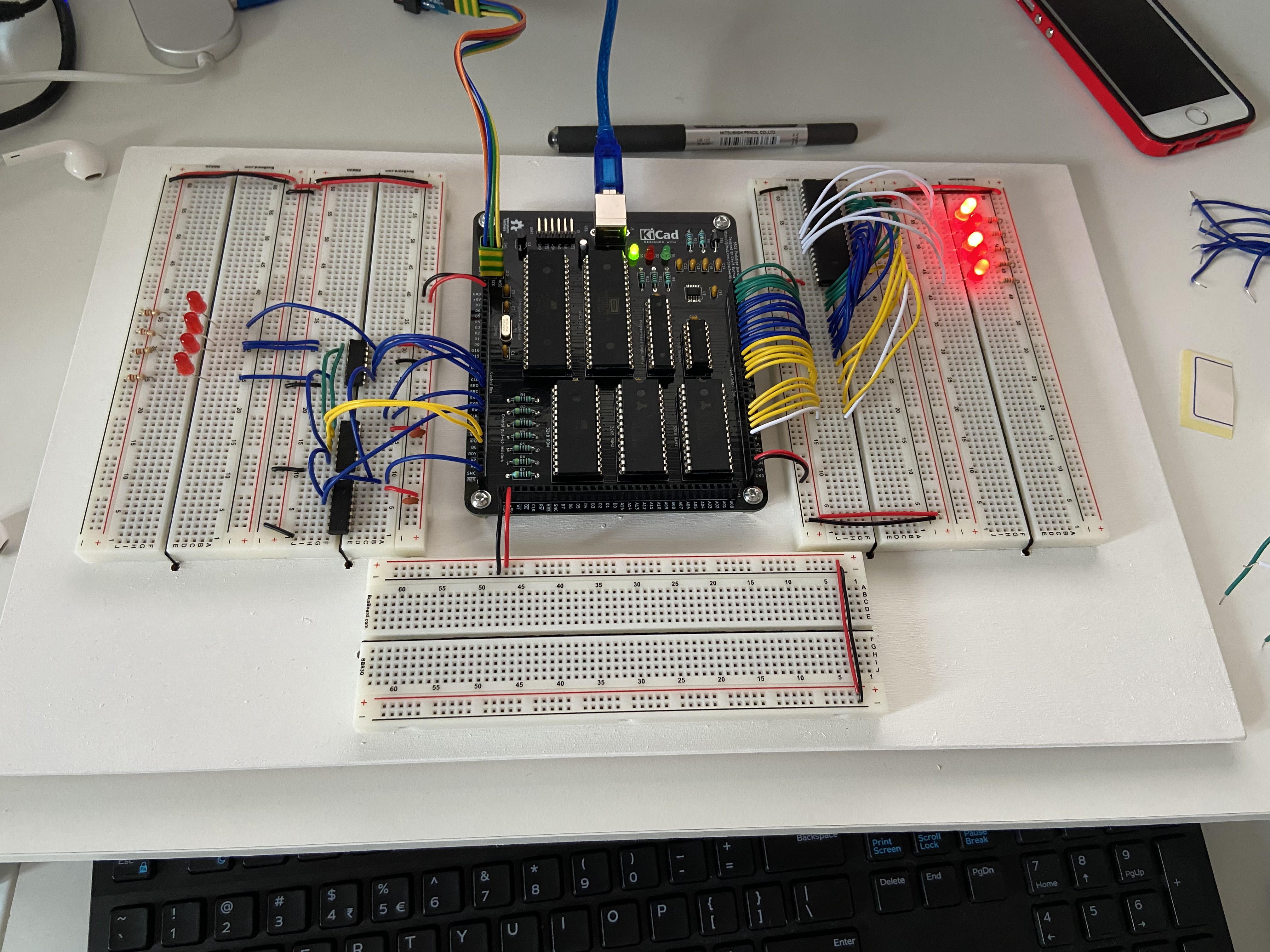
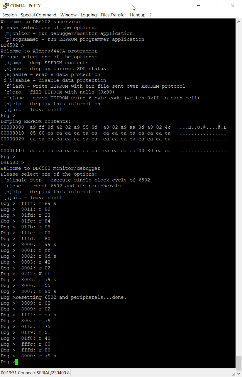
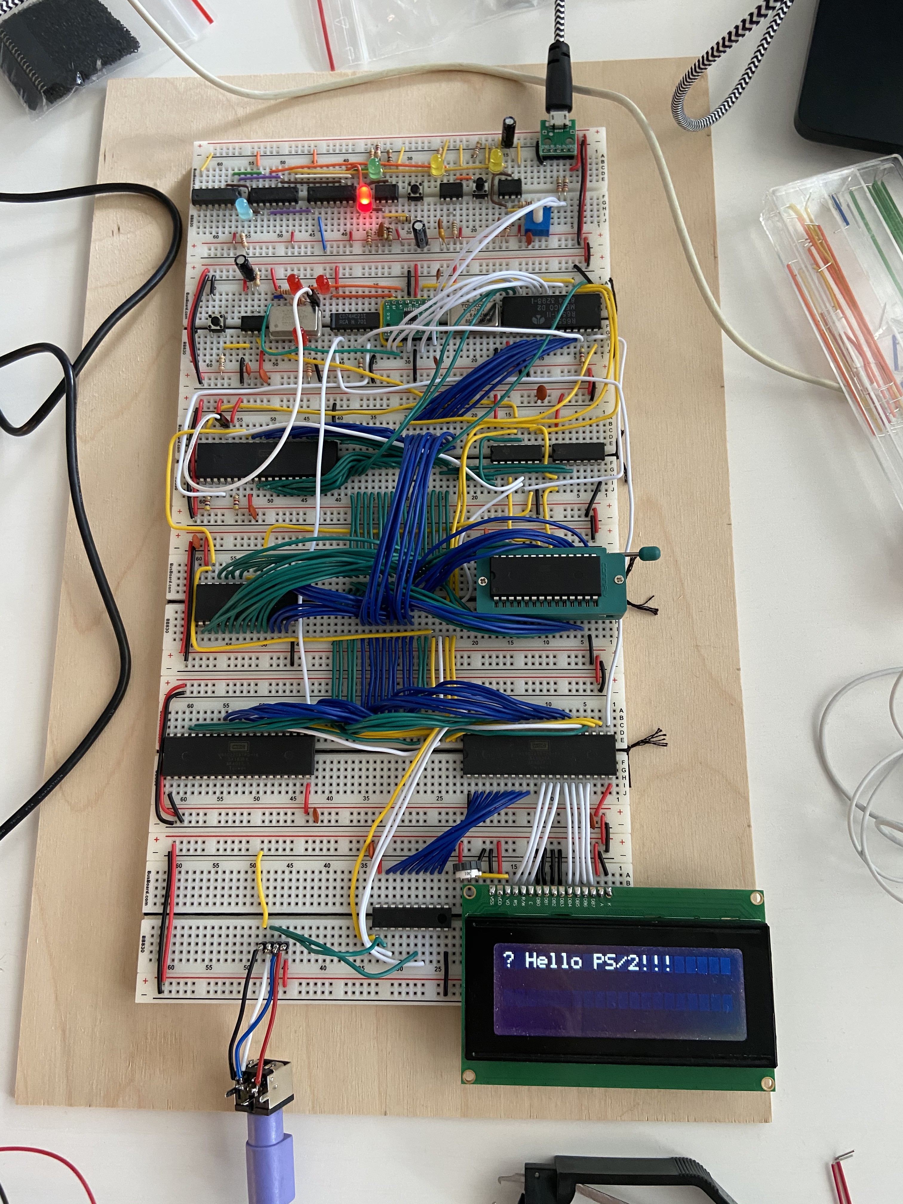
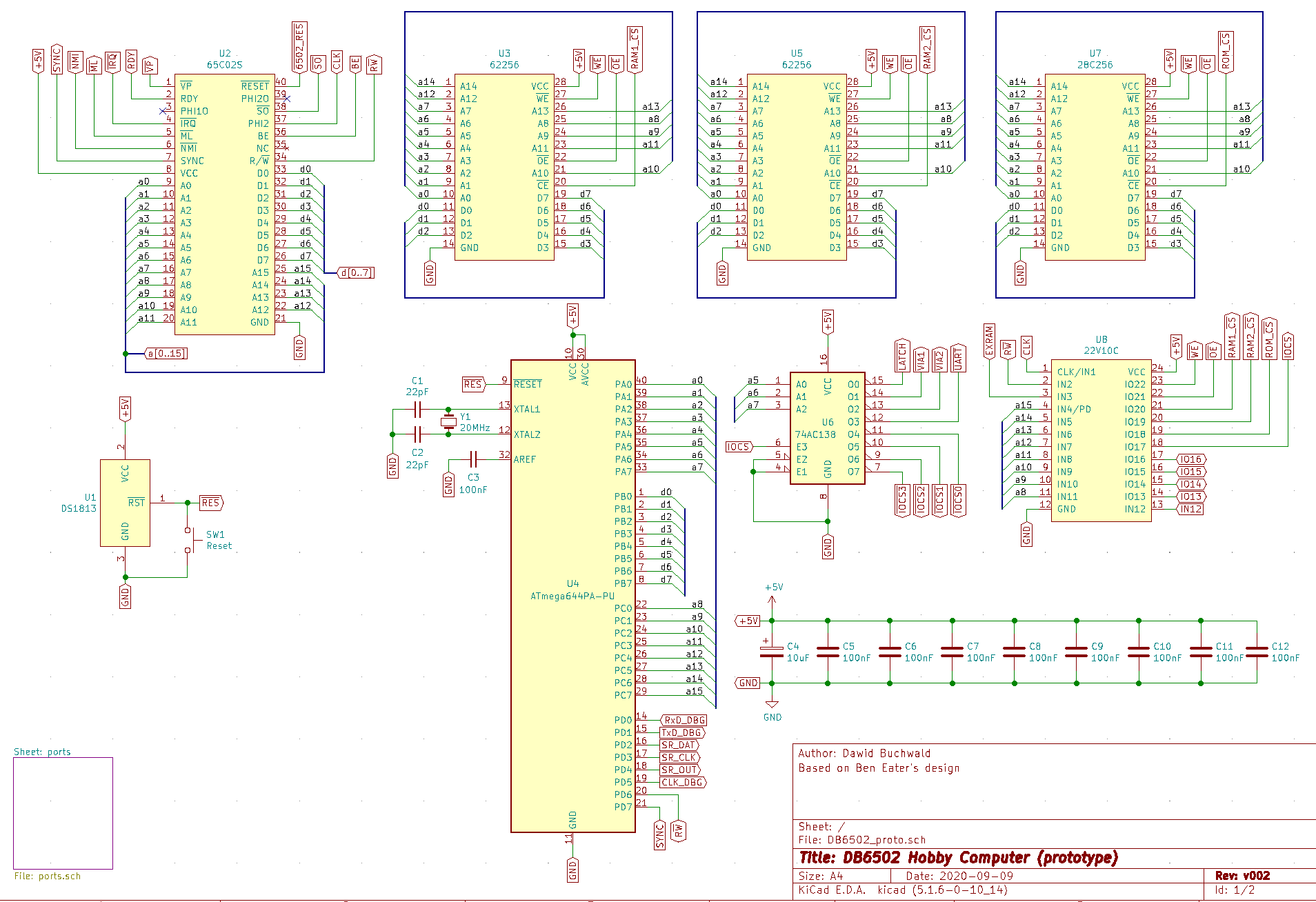
-
Wait states explained - 14MHz part II
12/16/2020 at 15:52 • 0 commentsHold your horses
Last time I wrote about three problems that one has to solve when trying to run 65C02 CPU at 14MHz. Obviously, how severe each of these is depends on the details of your build, so each case will be different. Let's start with comparison of two main methods and see how they can help you out with faster clock speeds.
One of the first issues you can think of (when looking at faster clock speeds) is the access time requirement for each of the components. When I started this investigation, I noticed that DIP package ROM chips were rated for 150ns access time - way too slow for anything above 4MHz.
Now you might wonder - I wrote in the past about my first build running at 8MHz - and you would be right, this was a mystery to me as well, and I will explain it later on. For now let's assume that access time is half of your clock cycle, and at 4MHz that would translate to 125ns - close enough for 150ns EEPROM to work properly at room temperature and stable 5V power supply.
So yeah, what are the options here?
The fastest 32KB one I could find was SOIC/TSOP/PLCC package 70ns access time AT28HC256 chip. You can go a little faster with AT28HC64 - it's 55ns, but only 8KB. If you want to compare these, you have to consider additional address decoding logic that will add to that, resulting in similar access time.
Still, even at 55ns you can't go much faster than 10MHz (half of clock cycle is 50ns), so what can you do about that?
Clock stretching vs. wait states
There are two ways to address this issue: one is not running your clock faster than the peripheral can handle, and this is called clock stretching; the other one assumes clock rate stays the same, but each CPU operation takes more than one clock cycle to execute. Hopefully the following diagrams should clarify the difference.
Clock stretching
Here is an example of clock stretching method:
We have two clocks: CLK1 running at 10MHz and CLK2 running at 4MHz. CLK is the actual clock fed to the CPU, and the switch always happens at low clock. Switch is triggered by address decoding logic circuit, specifically nRAM and nROM signals. Let's look at the sequence:
- At stage S1 it is assumed that previous access was also to RAM (so CLK1 is still being used). RAM is selected and CLK is fed from CLK1 source,
- At stage S2 full clock cycle has been executed (access to address 02FE), and following S2 ROM is being selected (CPU indicated it wants to access address FFFC), so CLK2 is to be selected. Since clocks must be toggled on target negative transition, there is a wait period until stage S3 when desired clock (CLK2) is going from high to low. In reality this is already part of the CPU cycle with access to FFFC,
- At stage S3 CLK is toggled to use CLK2 as source, and slow clock cycle is executed with access to FFFC address,
- At stage S4 slow clock cycle is completed, and CPU moves on to next cycle where RAM access is required. As previously, clock source can't be toggled until target clock negative transition (S5), but CPU already accesses RAM at 02FF,
- At stage S5 RAM access at address 02FF is performed with fast clock (CLK1) being CPU clock source,
- At stage S5 RAM access is completed.
As you can see, clock switching is not a trivial task, and if you are looking for a great document on how to implement it correctly, you will find it here.
Wait states
This is identical scenario, but implemented using wait states:
As you can see, there is just one clock here, CLK, running at 10MHz. I assumed that access time must be comparable to the clock stretching scenario, so the access time for ROM must be at least 250ns (full 4MHz cycle length), but please note: this assumption is actually silly, when you dig deeper into details. For now I just wanted to illustrate the mechanism.
So, the following things happen:
- At stage S1 CPU requests data from RAM (indicated by nRAM signal being low). Wait state generator circuit (responsible for determining how many wait states per device are required) will decide that there are no wait states required and memory can be accessed immediately, so the RDY signal is high,
- At stage S2 first CPU cycle is completed, and ROM access is requested. At this point wait states circuit determines that two wait cycles are required, and none has been executed so far, so the RDY signal is pulled low, resulting in CPU being held in current state and waiting,
- At stage S3 first wait state is completed, but one more is required, so RDY line is kept low for one more cycle, holding CPU in current state,
- At stage S4 second wait state is completed and this satisfied wait state generator requirements for ROM access, so the RDY line is pulled high. CPU executes the cycle as usual, but the previous two states allowed ROM to complete internal access operation,
- At stage S5 RAM access is requested, no wait state needed, so access is done in single clock cycle,
- At stage S6 RAM access is completed.
As you can see, wait states approach is a bit simpler, at least in theory.
How was it solved in the past?
So much theory, what about practice?
Actually the problem you are looking at is not new. Sure, we do have much faster chips nowadays, and, what's even more important, they are also much cheaper than they used to be, but problems rarely change over the course of history. When you check original Apple I manual, you will find there information about handling slow ROM access time (top left of page 12):
This wait state circuit explains clearly what needs to be done in case of slow ROM, but it fails to explains all the details of it - how it works, how it will affect the CPU and so on. It also uses PHI1O clock which, according to 65C02 datasheet, should not be used:
How does the wait state generator works? At each negative clock transition (PHI1O) 7474 chip (D-type flip-flop) will "remember" previous wait state. When accessing RAM, it doesn't matter (ROM CS line will be low, so the output from the 7400 NAND gate will be high, and such value fed into RDY input). When accessing ROM (ROM CS line will be high) and in previous cycle RDY was high the 7400 NAND gate will output low value and cause CPU to wait. In next cycle ROM CS line will still be high (it will not change, since CPU is waiting), but the output of 7474 will be low, resulting in high output from 7400 NAND gate.
Very simple, elegant solution, isn't it? Unfortunately, it can't be directly applied to 65C02 build.
Wait states explained
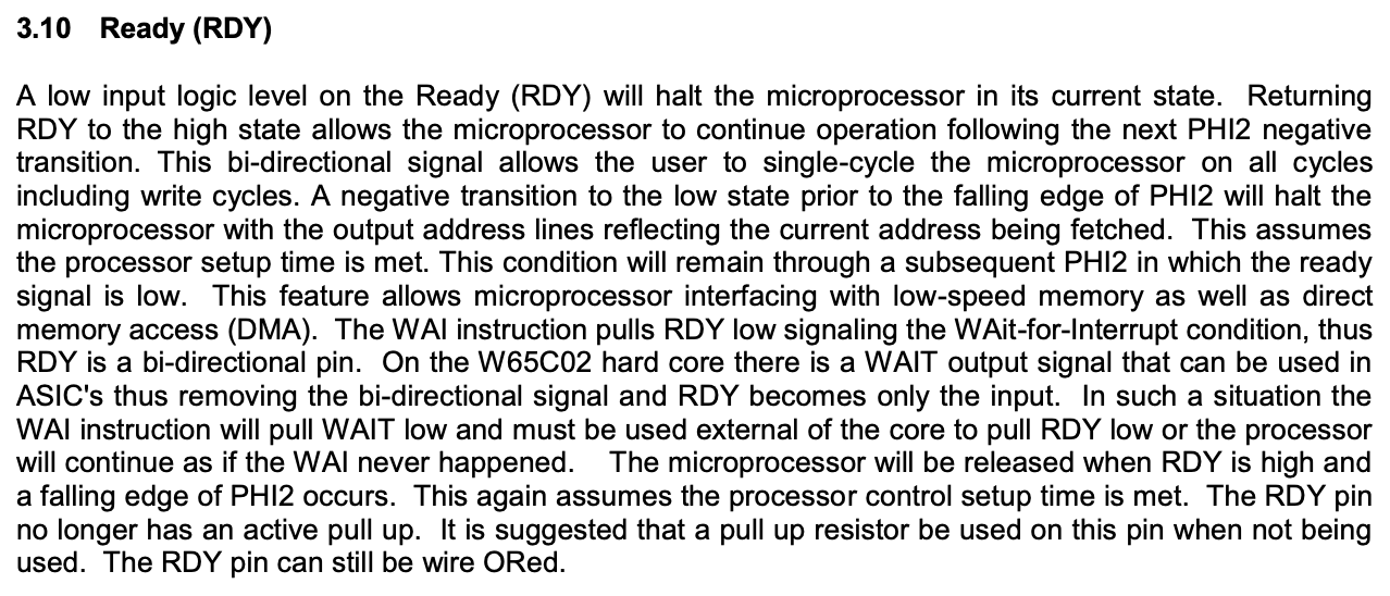
So, based on Apple I documentation we know that the slow peripheral issues can be addressed with RDY pin of 65C02 CPU. How to use it though? Official datasheet provides quite lengthy explanation:
I don't know about you, but I had to read it number of times and still it didn't make much sense. It has been clearly written by somebody who had quite complex context in his or her head at the time of writing, so let's try to take it apart and explain what these mean:
A low input logic level on the Ready (RDY) will halt the microprocessor in its current state.
OK, so low level on RDY will stop the CPU. How will it happen though? Will it be immediate, or will it happen at specific point in CPU cycle? As you probably know, there is a stage in CPU cycle when address bus is stabilizing at the beginning of the cycle - what happens if I pull RDY low then? Will it hold current (unstable) address or will it wait for it to stabilise and hold then? If you look at timing diagram, you will notice that it might have different effects depending on the point in time when the low pull happens - and the above description does very little to explain that.
Returning RDY to the high state allows the microprocessor to continue operation following the next PHI2 negative transition.
Ah, this is a bit more specific - returning to high state will not resume CPU operation immediately. At least we know from this part, that high level on RDY pin at any point in clock cycle will not have any effect until the very end.
This bi-directional signal allows the user to single-cycle the microprocessor on all cycles including write cycles.
This is my favorite part: three important bits of information mixed in one cryptic sentence that relies on broad context. What it means?
- This signal is bi-directional. This means that you can't assume this pin will always be input, and as a result, you can't always drive it unless you want to burn your CPU. There are some limitations - and they will be explained later,
- This signal has been used to single-cycle CPU in the past. Why? In his videos Ben doesn't use it, and single cycling works, right? Well, yeah, but the version used in the past (the NMOS one) didn't have static core. This means that it required constant clock operation to maintain its internal state. If you took NMOS 6502 version and ran it as Ben does it with infinite clock stretching, it would probably lose track of its registers. This is why in the past RDY was used to single cycle 6502,
- (...) all cycles including write cycles. - why is that even mentioned? Well, you probably know that the original NMOS 6502 version used the RDY pin only for read operation, right? Oh, you didn't? Yeah, neither did I, so I couldn't understand why this is being brought up here. The point is important when you look at older implementations - some of the old computers used clock stretching instead of wait states to drive slow peripherals, and this was the reason: NMOS version didn't allow for wait states during write operation, so clock stretching was the only option.
Sorry if it seems like I rant about the documentation, but I am. I understand that sometimes it's hard to forget all the context we have in our head, but seriously...
A negative transition to the low state prior to the falling edge of PHI2 will halt the microprocessor with the output address lines reflecting the current address being fetched. This assumes the processor setup time is met. This condition will remain through a subsequent PHI2 in which the ready signal is low.
Ah, so the low input on RDY (meaning "No, I'm not ready yet!") before the falling clock edge will halt the CPU with address lines set. Isn't that the same thing as in the first sentence? I don't know, I really don't.
The point here, however, is different: it means that if we keep the RDY signal low over the negative transition of the clock, the next cycle will keep the address (and data - in case of write operation) lines intact. It will be as if the following clock cycle was extension of the current one, and it will keep like this for as long as the RDY line remains low.
The part about CPU setup time you can find looking back at the diagram (tPCS at the bottom):
And how long is it? It should be no less than 10ns (assuming you are running 6502 at 5V):
So, we got another important clue here: the latest you can set the RDY low during clock cycle is 10ns prior to falling clock edge. Good!
This feature allows microprocessor interfacing with low-speed memory as well as direct memory access (DMA).
Ok, so it says that we can use it for interfacing with slow peripherals and it can be used for DMA. Slow peripherals - that's obvious, this is what we are discussing here, but how it translates to DMA?
Not that it's relevant here, but it makes sense to explain this here. RDY on its own is useless in DMA context. There is, however, another line that makes sense here: Bus Enable (BE). As it turns out, BE pin disables the bus control on 6502, but it doesn't affect CPU operation. If you pull BE down, 6502 will be disconnected from the bus, but from CPU perspective it will seem as if the bus was simply floating. It will still execute instructions, but they will be pretty random. This, obviously, doesn't make sense, so in order to execute DMA operation, one has to pull both RDY and BE low. BE to be able to drive the busses, and RDY to prevent CPU from going crazy in the meantime.
The WAI instruction pulls RDY low signaling the WAit-for-Interrupt condition, thus RDY is a bi-directional pin.
A-ha! So this is how RDY pin can become output pin! You might be wondering why it matters, but it does: if, for whatever reason, your 6502 encounters WAI instruction (even if it's not in your code, it might be in your data or in uninitialized memory, and in case of stack corruption data can get randomly executed), RDY pin will be driven low, basically shorting it to GND. If at the same time you are driving the pin high from your circuit (shorting it to +5V effectively), you end up having short between 5V and GND. This will result in excessive current flowing through the pin (and CPU) and might burn it. You don't want that, obviously.
Since you can't prevent WAI instruction from being executed, you have to prepare for that. There are basically two options here: use open-collector gate and pull-up resistor (open-collector gate will output only low signal or high impedance) or use series resistor between your circuit and the RDY pin. Both approaches are acceptable, but they have their own problems. I will discuss these below.
On the W65C02 hard core there is a WAIT output signal that can be used in ASIC's thus removing the bi-directional signal and RDY becomes only the input. In such a situation the WAI instruction will pull WAIT low and must be used external of the core to pull RDY low or the processor will continue as if the WAI never happened.
Now, I don't know what hard core model is, but I guess this is something different than DIP/QFP/PLCC package, because neither of these has the two additional lines. As a result this part is irrelevant.
The microprocessor will be released when RDY is high and a falling edge of PHI2 occurs. This again assumes the processor control setup time is met.
Is that about the hard core model or what? I have no idea. It seems like a repetition from before. I don't know.
The RDY pin no longer has an active pull up. It is suggested that a pull up resistor be used on this pin when not being used. The RDY pin can still be wire ORed.
Ok, so there is no internal pull-up on the RDY pin, so external one is needed when it's not used, just as in basic BE6502 build.
For the wire-OR of RDY pin, it's pretty obvious - as long as you use open-collector gates to provide RDY input signal, you can just wire-OR them, as any other open-collector signal.
Intuition vs. reality
So, after reading the datasheet you might be wondering when in the cycle should you toggle RDY signal low if your wait state generator circuit decides to put CPU on hold. When I was thinking about it initially I went with my intuition: RDY line should be pulled low during low clock phase (when CLK line is low).
This assumption was based on intuitive understanding of low/high clock cycle significance. The way I figured it worked was that low phase was the "preparation" and high phase was "execution". While this is mostly correct, it doesn't translate to RDY pin operation properly, and my intuition that RDY has to be pulled low or high during low CLK phase was just wrong.
Luckily I found this discussion on 6502.org - it shows interesting circuit, where RDY is asserted following rising CLK edge, so it definitely can be done later, even during high clock phase. Sure, it can't be done too late (see the note about Processor Setup Time tPCS above), but as long as it happens more than 10ns before the end of high clock phase, you will be fine.
Does it mean that you can decide high/low late during high clock phase then? Nope, not that easy...
Open collector issue
When you consider the implications of using open collector gate, you have to keep in mind interesting characteristic: while high to low transition is pretty instant (just a few ns fall time), the reverse transition is tricky and it depends on the value of pull-up resistor used.
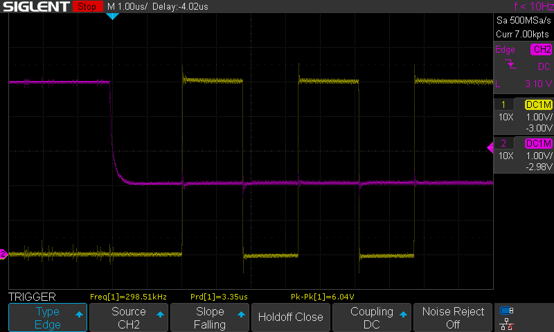
If you use anything in KOhm range, your rise time might be very, very long, like a 100ns. This is what I got with default 4K7 resistor I used:
Yellow line is the CLK line, and the pink is RDY line. As you can see, it took two full clock cycles (250ns) to rise to 5V. This means that wherever I was planning to use single wait state, I had two unintentionally...
On the other hand - use something very strong, like 50 Ohm and you might end up having problems with low signal being too high. It will probably take a few tries to figure out resistor value that will fit your scenario.
The other option (series resistor) is also discussed in the thread I linked above. Garth Wilson suggests to put pretty strong resistor (like 2K2) with 22pF capacitor in parallel. I haven't tested this approach, but I might have to. If I do, I will update this entry with the result.
Wait states summary
It might seem as the wait state approach is also pretty complex - but it's not in reality. It just takes a while to digest all this information and a bit of trial and error to figure out the implementation on your own.
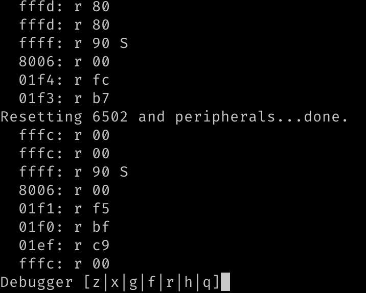
The good thing is that it can be implemented at any clock speed (even slow one), and it's really easy to troubleshoot using basic logic analyzer. This is sample reset sequence on my DB6502 build running at 2MHz with single wait state circuit for ROM access:
As you can see, there are three short RAM accesses, followed by two slow ROM accesses, then three RAM accesses and finally read of starting address from FFFC (8000). First instruction is also loaded, and it's opcode A2.
This also hints at another issue I will discuss in more detail later on - read/write signals stretching and bus interface translation.
-
The quest for 14MHz - part I
12/14/2020 at 19:52 • 0 commentsLong overdue update...
This update is long overdue - and apologies for that - but I have been really busy recently. Between family issues, failed parallel cooperative project, end-of-year workload increase and quite complex project challenge I found myself stuck, overwhelmed and demotivated to write.
Luckily things are looking much better now, and hopefully I can write more regularly now, because I do have quite a lot to share. It all started with simple challenge: run 65C02 (and the whole DB6502v2 build) at 14MHz. Simple idea, isn't it?
After all, this is the maximum CPU speed for which WDC 65C02 is rated for, according to official datasheet. Since I have already had it running at 8MHz in my first revision, it didn't seem like something very difficult to implement. Certainly not something impossible, but still, at the time of writing this words, I can't say that I have reached the goal fully. Sure, I did capture this nice screenshot (proving at least that it's partially possible):
![]()
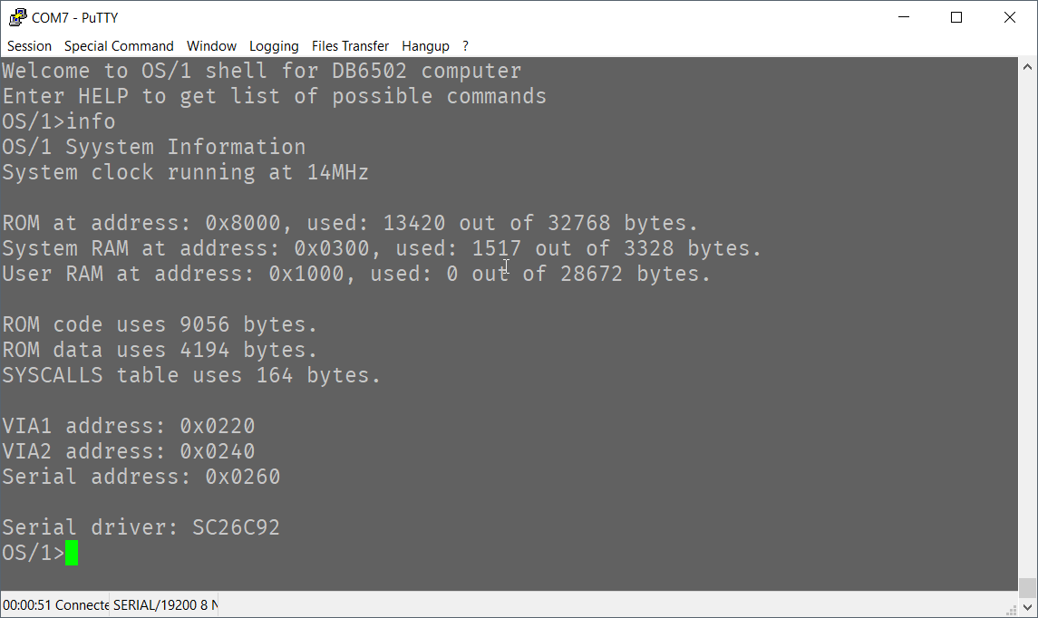
As you can see, measured and reported CPU speed is 14MHz and indeed it was running with crystal oscillator at 14MHz at the time. Was it stable? Well, one would say that any Syystem reporting its status like that is not very stable... Obviously, it's not a typo in the source code, it's a serial interface glitch resulting in double write.
So yeah, I have tried, but haven't succeeded yet. There are some other issues to handle, but I will write more about them as I describe the journey, as there is plenty to talk about. It will probably take a couple of project logs to go through it all. And to be fair, I might not even be able to get it to run reliably at that speed...
You might be wondering where's the problem - you just plug in faster oscillator and that's that, right? Well, not exactly.
How hard can it be?
Famous last words.
Unfortunately, as we all learn when pushing the limits of our unconscious incompetence, it usually is harder than it seems. Sometimes it might seem like making one more step should not be harder than those previously made, but life can surprise us in all possible yet unexpected ways.
As I wrote in previous logs couple of times, this adventure of electronic discovery has been full of surprises and weird glitches that could have been perfectly well explained if only investigated closely enough. Sometimes these glitches are infuriating, making even the best theoretical circuits fail in unpredictable ways, and sometimes they seem like miracles that I took for granted.
Let's look at the three main problems that I have encountered during my journey.
Problem 1: timing
When you look at datasheets of various components, you will notice that they have pretty strict limitations in their timing. 28C256 EEPROM in DIP package (used in Ben's build as well as mine) is rated for 150ns access time. I wrote about it some time ago, when I was surprised I got it to work at 8MHz - and right now I understand much better what happened back then, but the general idea is that when your clock speed increases more and more challenges emerge.
Let's consider address decoding for instance: when you are operating at 1MHz your full clock cycle takes 1000ns, and
![]()
It might seem like a really short time (30ns max vs. 1000ns cycle time), but when you consider that at 14MHz each clock cycle takes only 71ns, it suddenly becomes major concern. Each single nanosecond counts and matters.
So yeah, not only RAM access time is an issue here, everything can cause problem.
Funny thing is that even the "fast" SRAM used in Ben's build (62256) is not fast enough for anything above 9MHz with its access time of 55ns - and it took me a while to figure that one out as well...
To summarise: first main problem is how fast everything happens at 14MHz, and how to manage this speed.
Problem 2: documentation
To be fair, this might be my issue only, but I found the
![]()
And, as it turns out, this was just the beginning - there are many small details here that need careful consideration. Again, not a problem for moderate CPU speed, but at very tight timing it does matter how you do it.
Problem 3: CPU families and interfaces
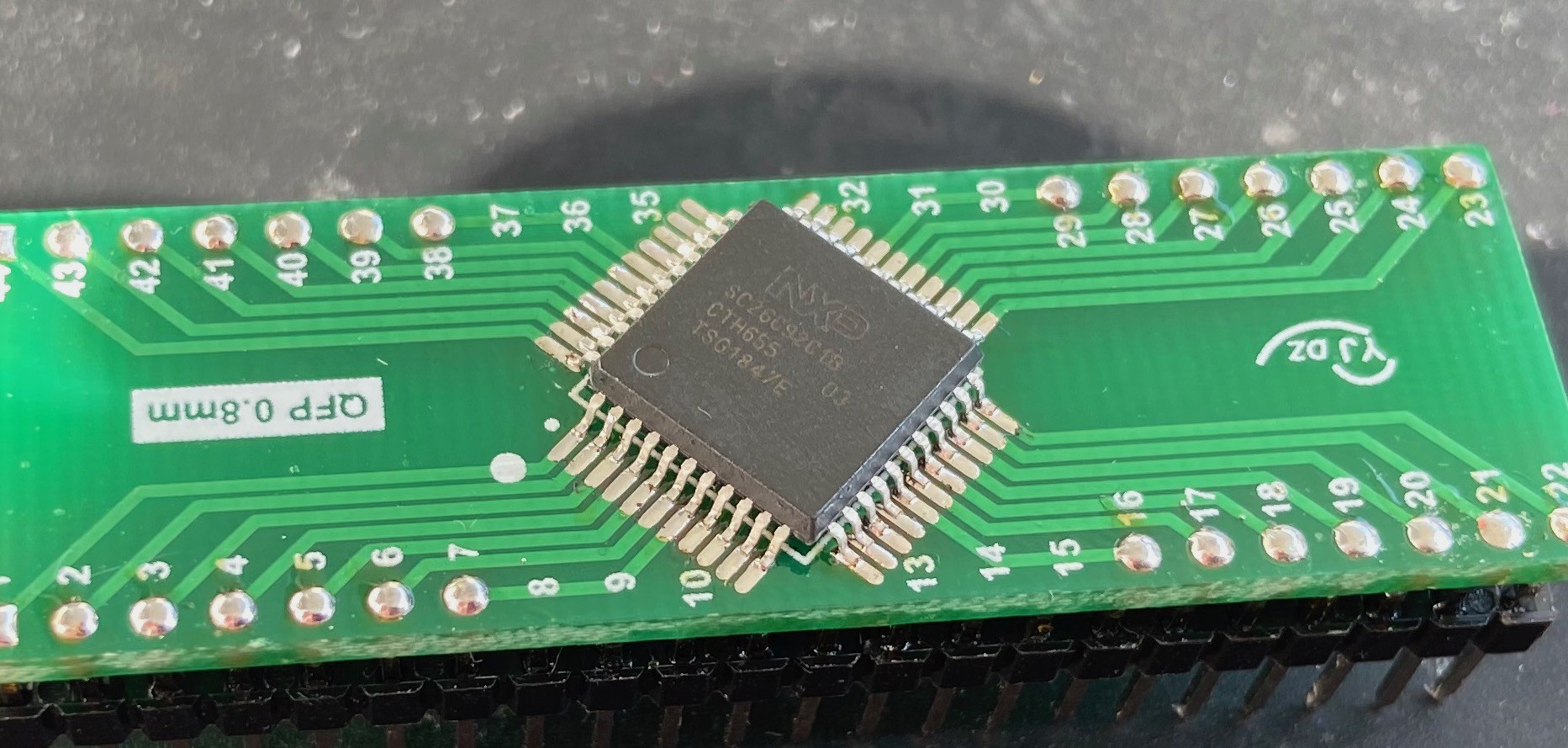
This is something I've been meaning to write about for a long time, practically from the day I left the safe and cozy world of 65XX family of peripherals. Sure, one could argue that even the ROM/RAM chips used in Ben's build are not fully 65XX compatible, but using chips like the 26C92 UART controller (especially at higher clock speed) becomes interesting challenge on its own.
I mentioned another parallel project I've been working on, and it has been really interesting for one specific reason: I used Z80 CPU for it and I strongly recommend you take a look at this one some day. There is no shortage of projects similar to BE6502, but based on Zilog CPU, and it's really interesting to compare different chip philosophies. Noticing these differences first-hand can really deepen your understanding of computer system architecture.
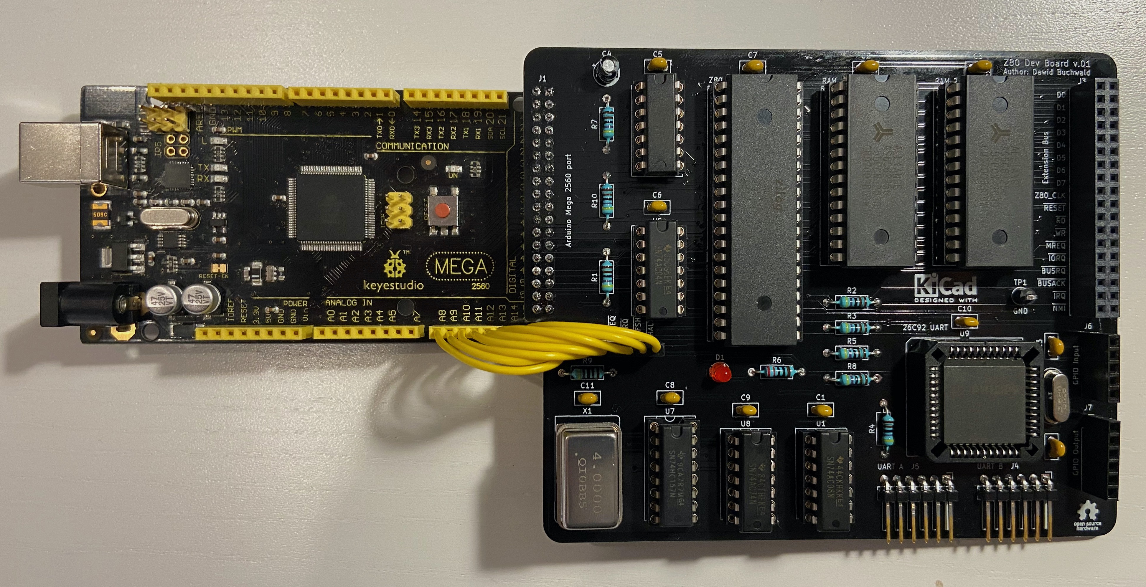
And while it's not really relevant to what I'm writing here about, as a side note: I will probably revive my other project one day, for now I have very convenient Z80 RAM-only, Arduino Mega compatible development board with dual channel serial interface:
![]()
I will write more about this one day, but for now it's just a nice reminder of what can be done in short amount of time and not that much effort.
Bottom line: while it doesn't matter much at lower clock speeds, translation from 65XX bus to 8080 bus at higher frequency can present interesting challenge and cause completely different set of issues.
Summary
-
Another fascinating glitch!
10/27/2020 at 10:23 • 1 commentWhy this keeps happening to me?
So, last time I wrote about things that scare me the most: some seemingly random glitches that obscure larger design problems. This is why whenever I see something off I get really anxious - I'm afraid this time it will be too hard to fix, and I got pretty terrified recently!
As usual, I want to share the story, partially because it makes for a nice cautionary tale, and partially because it was pretty interesting investigation that followed, with some magical twist to it.
Status update
First things first, to set the stage. Recently I made an amazing discovery, but I will cover this in a separate entry. Suffice to say I managed to solve one of the major pains with my first version of the board without any significant modifications to version 2.
As a result I could finally move forward with clock switching design I wrote about previously. After having included all the comments from Reddit, I moved on to hardware implementation: one 74AC74, one 74HC157 and a full-can crystal oscillator.
I was surprised to see how easy that was. With all the schematics prepared in advance and prototype build for my test fixture it took less than 15 minutes.
Booted up OS/1 and all seems fine, the whole machine started at 8MHz, ran just fine until I decided to enter debug mode where it seamlessly switched to 300KHz mode with bus logging and when needed I could single step down to half-clock-cycle precision. Lovely.
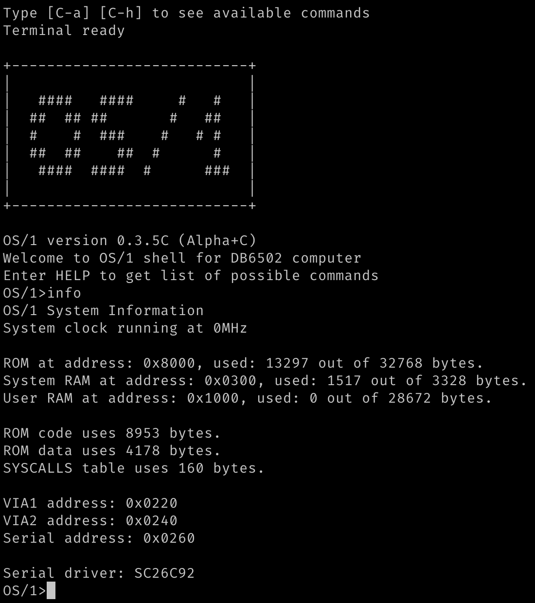
Another feature I included was real-time CPU clock frequency measurement, so the below output was captured in a single session, without restarting or powering down the computer:
+---------------------------+
|                           |
|   ####   ####     #   #   |
|  ##  ## ##       #   ##   |
|  #    #  ###    #   # #   |
|  ##  ##    ##  #      #   |
|   ####  ####  #      ###  |
|                           |
+---------------------------+

OS/1 version 0.3.5C (Alpha+C)
Welcome to OS/1 shell for DB6502 computer
Enter HELP to get list of possible commands
OS/1>info
OS/1 System Information
System clock running at 0MHz

ROM at address: 0x8000, used: 13420 out of 32768 bytes.
System RAM at address: 0x0300, used: 1517 out of 3328 bytes.
User RAM at address: 0x1000, used: 0 out of 28672 bytes.

ROM code uses 9056 bytes.
ROM data uses 4194 bytes.
SYSCALLS table uses 164 bytes.

VIA1 address: 0x0220
VIA2 address: 0x0240
Serial address: 0x0260

Serial driver: SC26C92
OS/1>info
OS/1 System Information
System clock running at 8MHz

ROM at address: 0x8000, used: 13420 out of 32768 bytes.
System RAM at address: 0x0300, used: 1517 out of 3328 bytes.
User RAM at address: 0x1000, used: 0 out of 28672 bytes.

ROM code uses 9056 bytes.
ROM data uses 4194 bytes.
SYSCALLS table uses 164 bytes.

VIA1 address: 0x0220
VIA2 address: 0x0240
Serial address: 0x0260

Serial driver: SC26C92
OS/1>
First time the INFO command was invoked, the computer was running at 300KHz, hence the 0MHz reading. Before second invocation I switched clock in the supervisor session to 8MHz and it was detected properly as you can see above.
Lovely, isn't it?
It seems like more and more features from my dream DB6502 build are getting implemented nicely, I'm proud to report :)
And then it happened...
So, obviously, I needed to test some more complex programs to see if the system is stable. I mean it's all very nice, but bare operating system doesn't make for a good testing software.
I loaded some simple programs, and they all worked just fine. Tried MicroChess, which is using CPU and memory extensively and this one also worked correctly, no glitches there.
Time for the most difficult one: Microsoft BASIC interpreter. It loaded just fine (well, almost, but that is different story I will cover another time), and I ran it in anticipation. It starts by asking user if this is Cold or Warm boot, and depending on the answer it starts memory size detection routine.
The "memory detection" is really simple mechanism: it starts from defined address and moves on, byte by byte, writing and reading 0x55/0xAA to each address. When the read matches the write, it means that particular address is in RAM. Obviously, ROM is not writeable, so the write doesn't succeed and the value that is read back doesn't match the intended write.
Unfortunately, this hasn't happened. Computer just froze, and after getting into AVR debugger I noticed that it simply ran into 0xDB (STP) opcode at some random ROM location and just hang up. It was now up to me to find how it got there in the first place.
Needless to say, it all worked just fine on the first revision of my computer, so the code as such, was perfectly fine.
This is why I designed version 2 in the first place!
Well, this is exactly this kind of thing I built my DB6502v2 for, right? To be able to troubleshoot such issues much better. So, I reset the machine, loaded MS BASIC again, toggled to "bus analysis" mode with 300KHz clock and ran the software again, hoping to see where it fails.
Thing is: it didn't. It just happily went through, found out that ROM starts at 0x8000 and moved on to the proper MS BASIC prompt, where everything worked just fine.
F**K.
There is not much use of debug mode if it works differently from the non-debug, right?
I was really upset at this point, and since last couple of days were a bit depressing overall (COVID-19 explosion in Poland, political turmoil around women's rights movement), I was really considering just giving up here. I was afraid this was the point where I was in over my head finally. Depressing.
The main problem with all these cases is that I'm afraid this will be something really, really difficult to find, let alone even consider fixing it. The worst part is something like IC timing violation. I already know you can do it and get away with it: after all, my DB6502 version 1 runs at 8MHz with 150ns ROM. Never had any problems with it, but it also means that you can violate IC timings and not notice that immediately, leading to more and more problems in your build and making them less and less likely to occur in single place. These things scare me the most. I just didn't have that in me to continue at this stage.
Decided to spend some time with my family, take my mind off these things. Let it brew inside, but redirect the focus. Couple of hours later, when I was reading another story about Chase of Paw Patrol rescuing Chicaletta, it struck me. I had some idea what could cause this, and, strangely enough, as it turned out couple of hours later, this intuition was spot on. It did take me quite a while to confirm the suspicion, but it was simple problem afterwards. I will hold on to the hypothesis for now, to let you figure it out on your own.
Logic analyzer to the rescue!
So, if I can't use the debug mode of my supervisor, maybe I can catch the problem with my logic analyzer then? Sure, it's not as friendly to use, but still, maybe I can get the data out of it?
There is, however, "small" issue here: I need to gather data from quite a long operation, at high frequency (at this point I changed crystal to 1MHz, and confirmed it also failed with it), and my view is quite limited: I have only 16 lines, and I need to observe full data bus (8 lines), clock, R/W, nWE, nOE and some other signals. All I can look at is just three-four address lines, which is not too much.
And, on top of that, how to read this crap? Couple million entries, and all I have is 0 or 1. All I have to do is to find the single one that causes the failure. Good luck :)
I wrote about it some time ago - I got myself pretty cheap (120$) 16-channel 200MHz KINGST LA2016 logic analyzer. Comparable devices from the major brands are several times that. The issue, however, is that PulseView software doesn't seem to like that device, and the official software is pretty limited. Or, so I thought.
For the first time I started digging deeper into the decoding section, as it never seemed that useful. It lists RS232, CAN, LIN, SPI, I2C and that's it. Oh, wait, there is "other analyzers..." menu item I haven't noticed before.
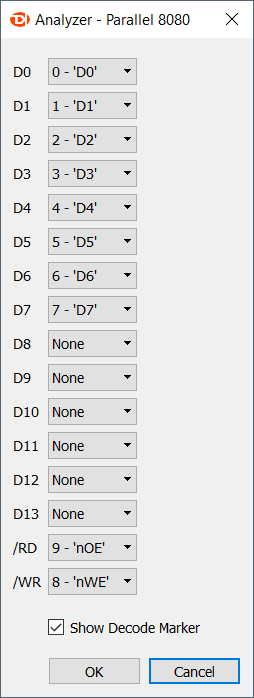
BOOM. Parallel 8080!
Check out this bad boy:
![]()
This is literally EXACTLY what I needed. Suddenly it turned out that analysis might be much easier after all!
The data in question
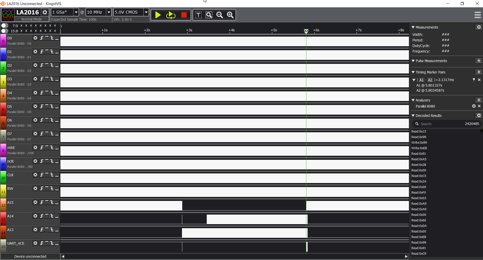
So, this is what I have to work with:
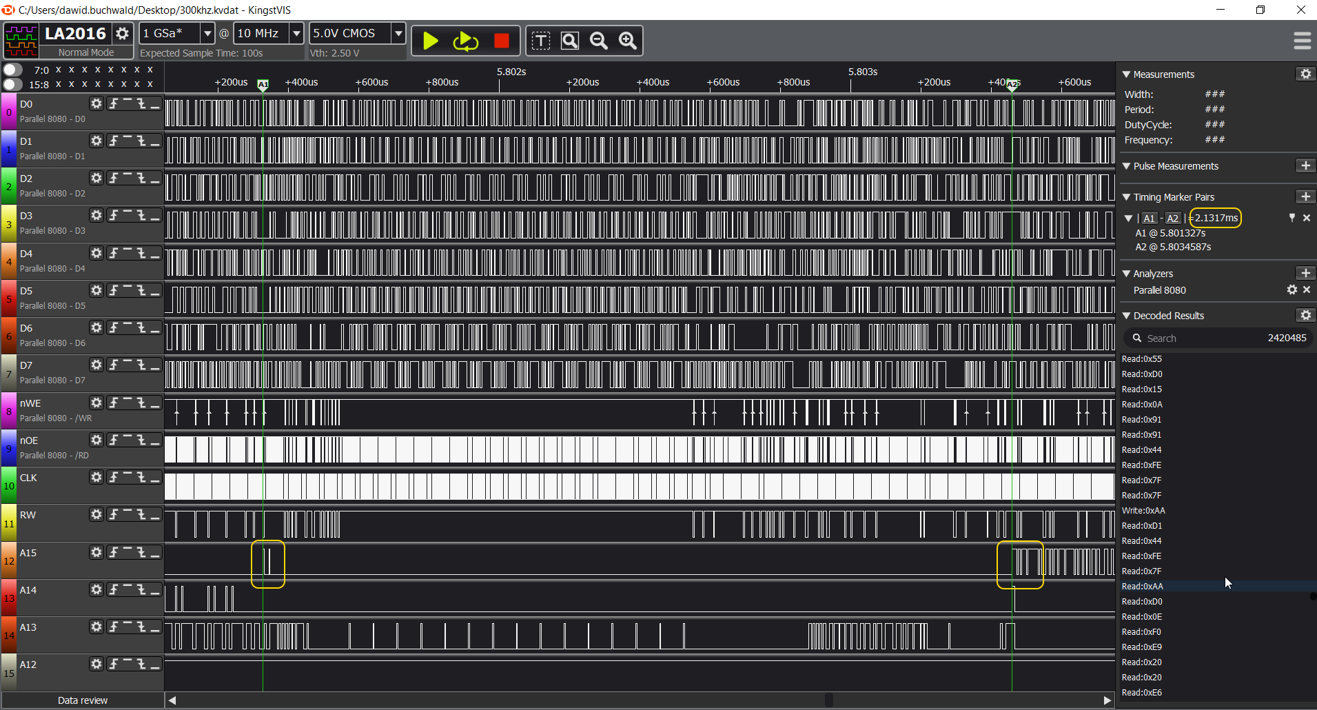
![]()
PLEASE NOTE: I will start with showing the correct result, captured during execution at 300KHz and move on to incorrect one, captured at 1MHz.
From top-level view you can already see interesting pattern: the middle section (where A15 is low) is probably the memory probing routine. Let's verify by zooming in:
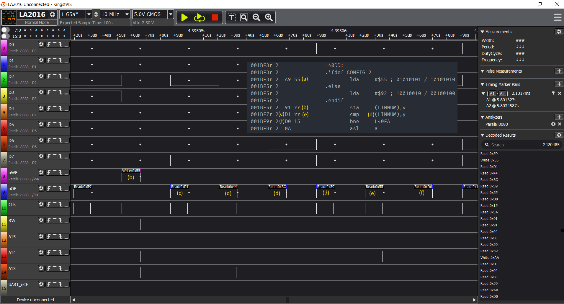
![]()
Please, open the image in new tab to follow the description:
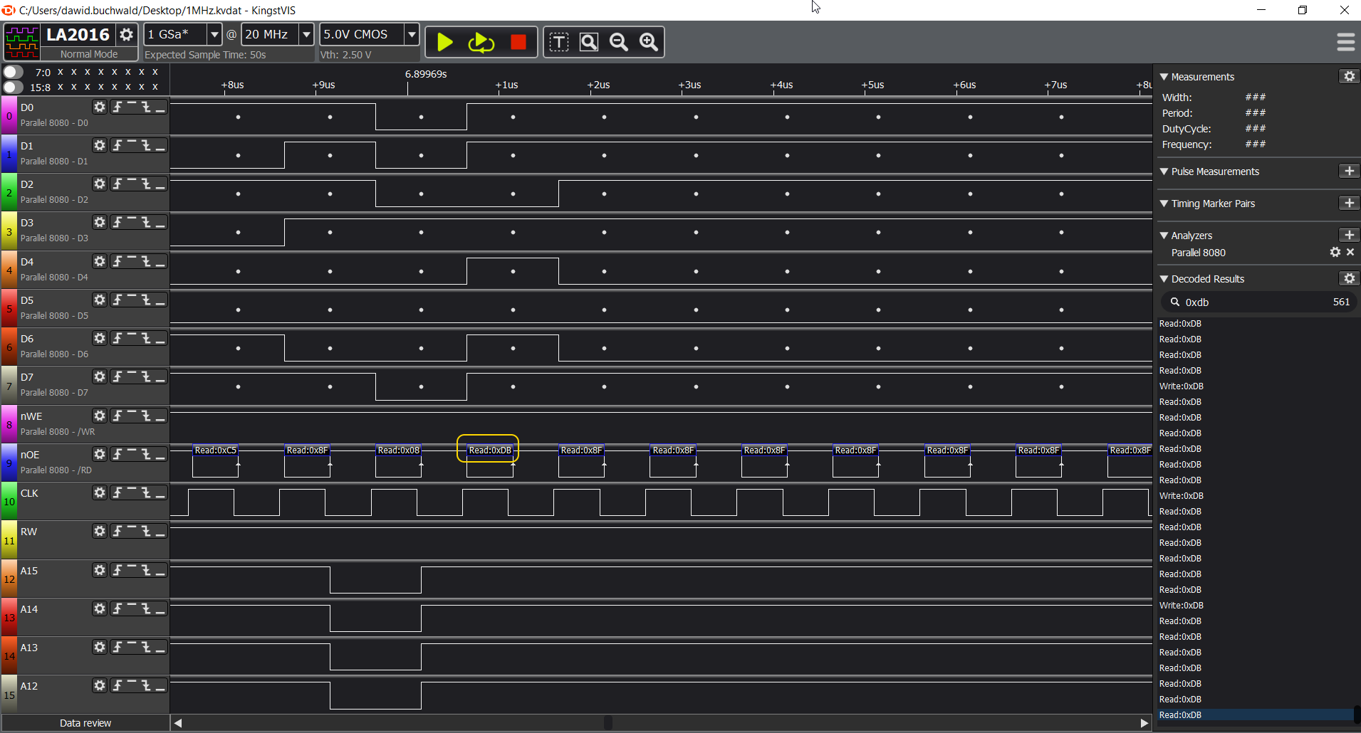
- (a) value 0x55 is being written to some memory address (0x598C - will explain below), but we can't see the actual 0x91 (STA) opcode here (b), only the execution result which is write to RAM cycle,
- (c) first operation following the write is read operation from the same address. Since we are using indirect ZP addressing here, and LINNUM is mapped to address 0x0044,
- (d) we are reading target address from location 0x0044 and 0x0045 - and the address is 0x598C),
- (e) we are reading value from address 0x598C which is 0x55 - exactly the same value we wrote there, so this is still RAM.
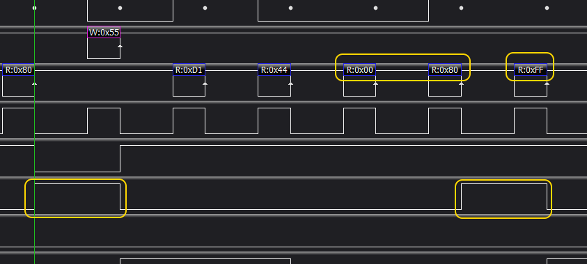
Next step is to verify what happens at the end of RAM and beginning of ROM:
![]()
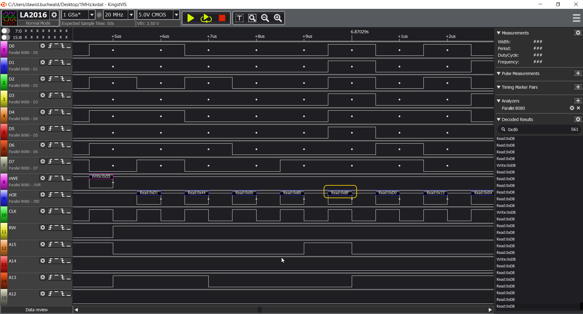
So, comparing to similar RAM cycle above, we can see the two main differences:
- first, the A15 address line is high for the write access, meaning we are now writing to ROM, not RAM,
- second, the value read back from the ROM (at address 0x8000) is not the same as value written to it (0x55), indicating that we have reached non-writable memory here.
OK, we have correct output, let's see the incorrect one.
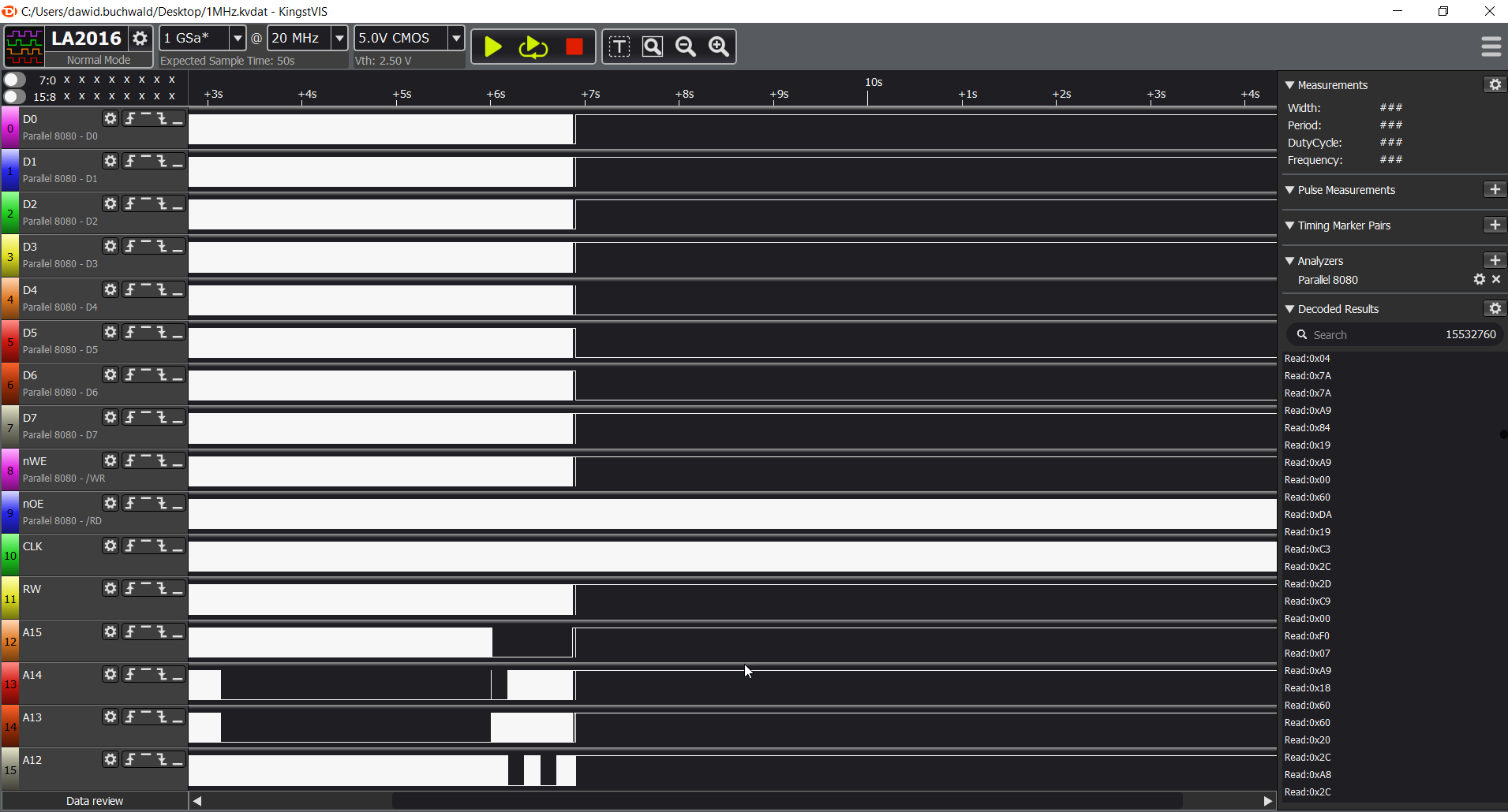
Incorrect run capture
First thing that you will notice is that the failed execution looks quite differently:
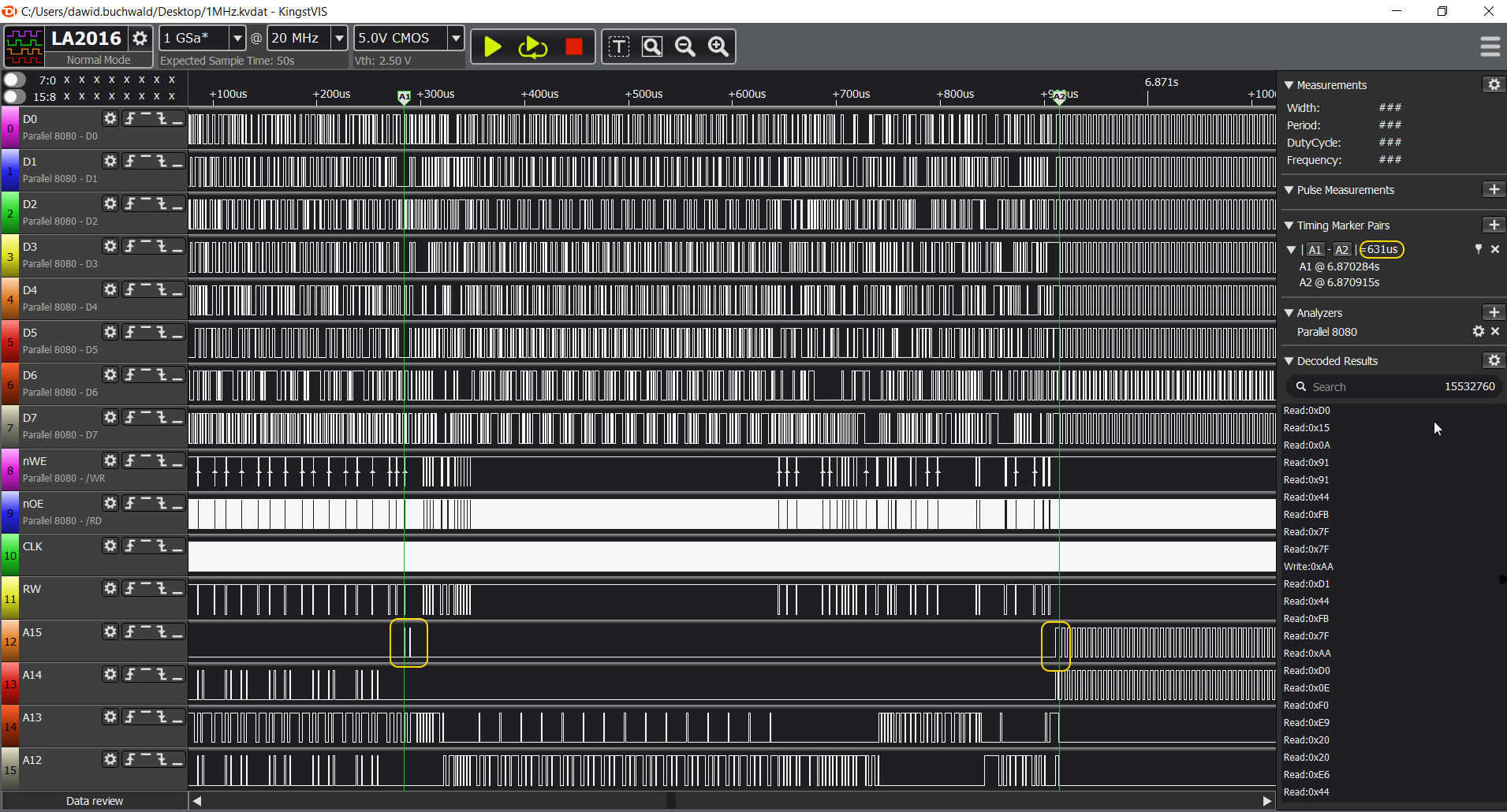
![]()
Sure, we have the memory probing section, but what happens immediately after doesn't look very good, and it's not that similar. Let's see what's happening there.
Just at the edge of the "busy" section, we can see that:
![]()
Yeah, STP opcode and nothing but black death afterwards.
Let's rewind back to the memory probing routine:
![]()
Seems like it worked its way up to 0x8000, where it detected non-ROM location. Check out the screen and think for a second. Spoiler alert: upcoming hypothesis!
What was it then?
In case you missed it, previous time the value read from 0x8000 was different, although it was the very same ROM.
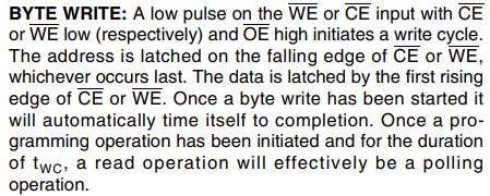
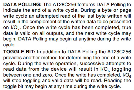
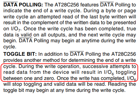
So, when reading bedtime story for my son I suddenly remembered interesting feature of the ROM chip: when you write to it, you can check for completion of write cycle by reading back from the last written address. As described in datasheet, it will respond with seemingly random values, but in fact it will be sort of "tick-tock" counter:
![]()
![]()
And, since it's ROM memory with enabled Software Data Protection (my AVR uploader enables it every time after flashing for protection against inadvertent writes), the write as such will not happen, obviously, but maybe the ROM is waiting for something?
So, the hypothesis was: everything is working fine, but following the write operation to first ROM address, all the successive reads from it will fail, resulting in corrupted data.
That explanation seemed perfect, because it addressed all the observations made so far:
- First version of DB6502 had the nWE line of ROM tied high, so the "write" operation to ROM was not really happening, and the ROM didn't initiate write cycle,
- It worked just fine on the slow clock (300KHz), because there was enough time for ROM to complete "write" cycle,
- It failed on 1MHz and faster clock because there was not enough time for the write cycle to complete.
There is, however, significant issue with the hypothesis: even if that happens, we are not reading the same location of ROM as the one we wrote to, so the "data toggling" should not happen. Or, maybe I'm reading the datasheet wrong?
So, let's test this hypothesis then. Let's go back to the correct run analysis:
![]()
I marked two consecutive accesses to ROM. First one is the failed write, and the next one happens just over 2ms later. Most probably this is MS BASIC calling some OS/1 routine from ROM to display characters on the screen or something.
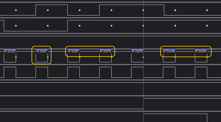
Let's zoom in on the second access:
![]()
Yeah, exactly. What you can see here is that we have JMP (VECTOR) opcode (0x6C) reading the VECTOR address from ROM address 0xF89C. This is exactly the memory range where OS/1 keeps system routines vectors, and as you can see, it results in a read of address 0x9AAB, which, most likely, is ROM address of some OS/1 function.
Now, let's compare that against the incorrect 1MHz execution capture:
![]()
We have the same pattern: write access to 0x8000, some processing in RAM (actually this is where MS BASIC calculates amount of available RAM memory and converts it into floating point decimal value), followed by another ROM access, but considerably faster, after some 631us.
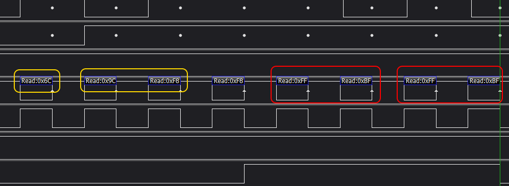
Please keep in mind that this second access should yield the same result, as it accesses the same address in the same ROM. Let's check then:
![]()
BOOM!
Instead of valid address (0x9AAB) we are getting 0xFF/0xBF, which is exactly the TOGGLE BIT thing that the datasheet talks about:
![]()
Now, I don't know really how many times I have read this datasheet, but it was many, many times. I had to understand the mechanism correctly to implement super-fast EEPROM flasher in my AVR supervisor software, and I did struggle to get it right.
So, important lesson learned here: taking time off, spending time with family and letting your mind wander can work miracles. And, datasheets contain probably all the information you need to succeed with your build, it's just that we might miss it the first hundred of times reading it :)
Have fun, stay safe and please, let me know what you think in the comments below!
-
Test Driven Development meets hardware
10/20/2020 at 20:01 • 0 commentsThe scary stuff...
So, I don't know about you guys, but for me the most scary part about designing any circuit whatsoever is that it might not work, but not all the time, just every now and then. Failure rare enough to be near impossible to capture, yet severe enough to make the device unusable.
Sure, you can test your design all you want, but honestly, how many reliable tests can you execute? What if the problem is related to one of the most heavily used parts of your circuit? That will be near impossible to troubleshoot.
So, I came with an idea for DB6502 v2 that would enable two modes of use: full-speed mode, without AVR supervisor attached (say 8MHz, will go faster next time), and slow-speed mode, with AVR analysing system busses. Obviously, AVR would be controlling the selector, and user can choose the mode on the fly, via the supervisor shell.
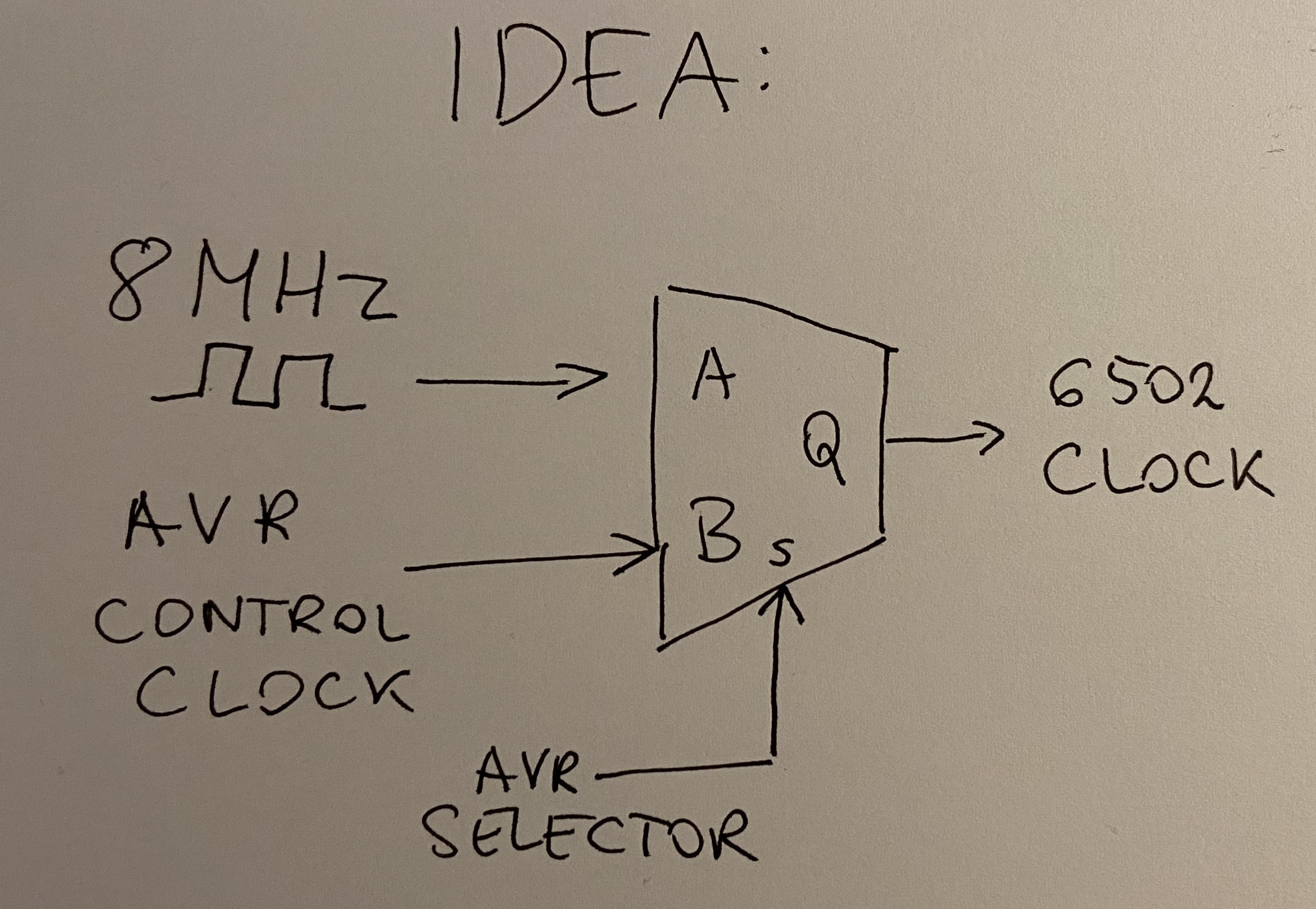
Implementation of such contraption is actually pretty simple - all you need is single 2:1 multiplexer:
So, depending on the signal fed to S pin on the mux, 6502 would be fed with 8MHz clock or the slow AVR variant. There is, however, a serious problem with this approach:
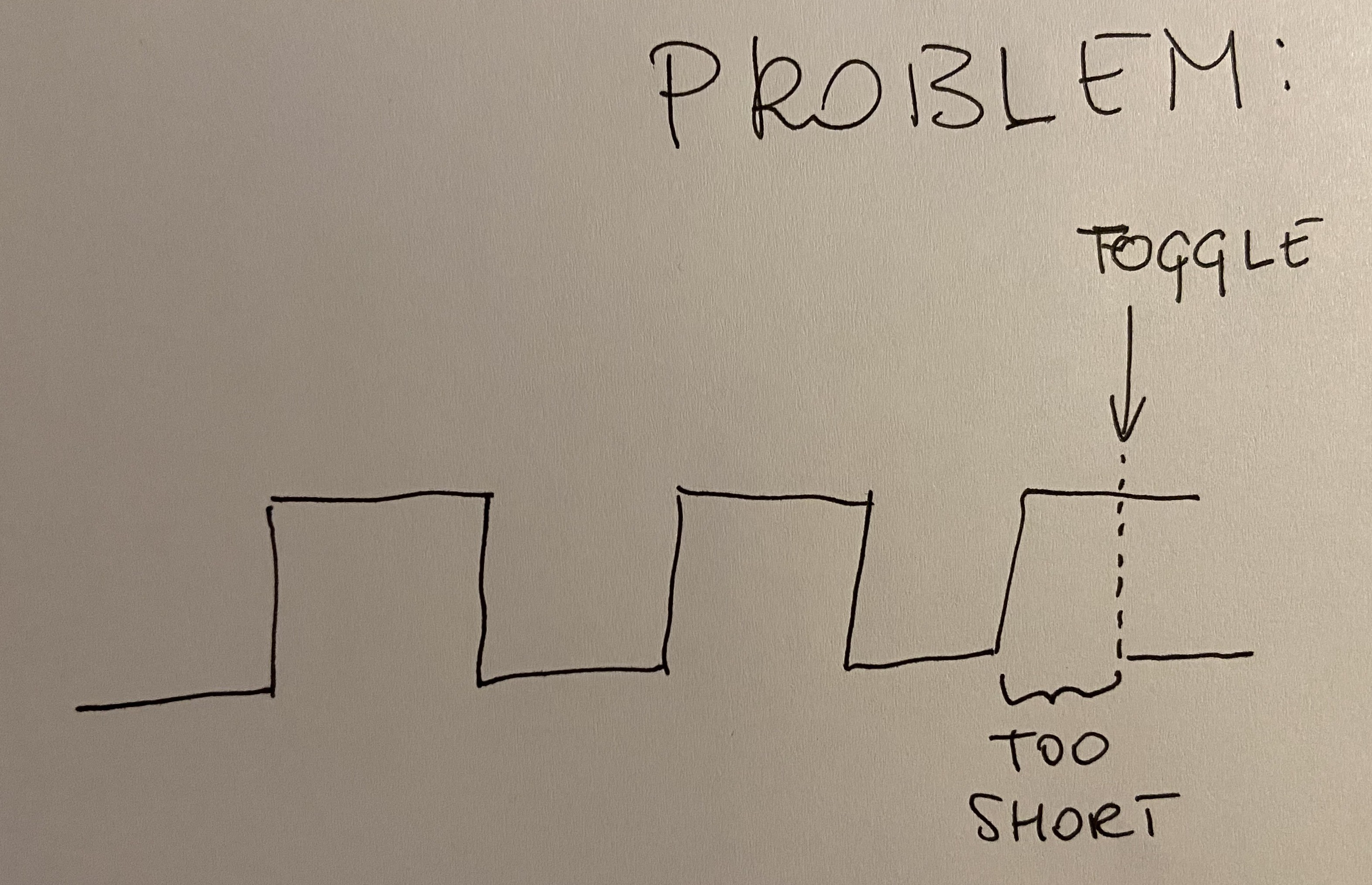
There are certain requirements in the 6502 CPU as to the length of the clock cycle. Both high and low phases of the clock need to be of certain duration. If the toggle happens in the middle of low or high phase (called PHI1 and PHI2 respectively), CPU state might get corrupted. Nothing tragic, but whatever software ran on the computer would no longer work as expected.
Probably most of the times you wouldn't even notice, because CPU would somehow recover or the data that was corrupted (like accumulator state) was not important (as it was going to be overwritten anyway in next cycle).
However, every now and then, the results would be catastrophic - execution would fail due to hard to pinpoint glitch.
The problem is that you need to find a way to ensure these things don't happen. Even if you know what to do (and probably some of you already know the solution to the issue at hand), the important questions is: how do you know the solution will work?
TDD to the rescue!
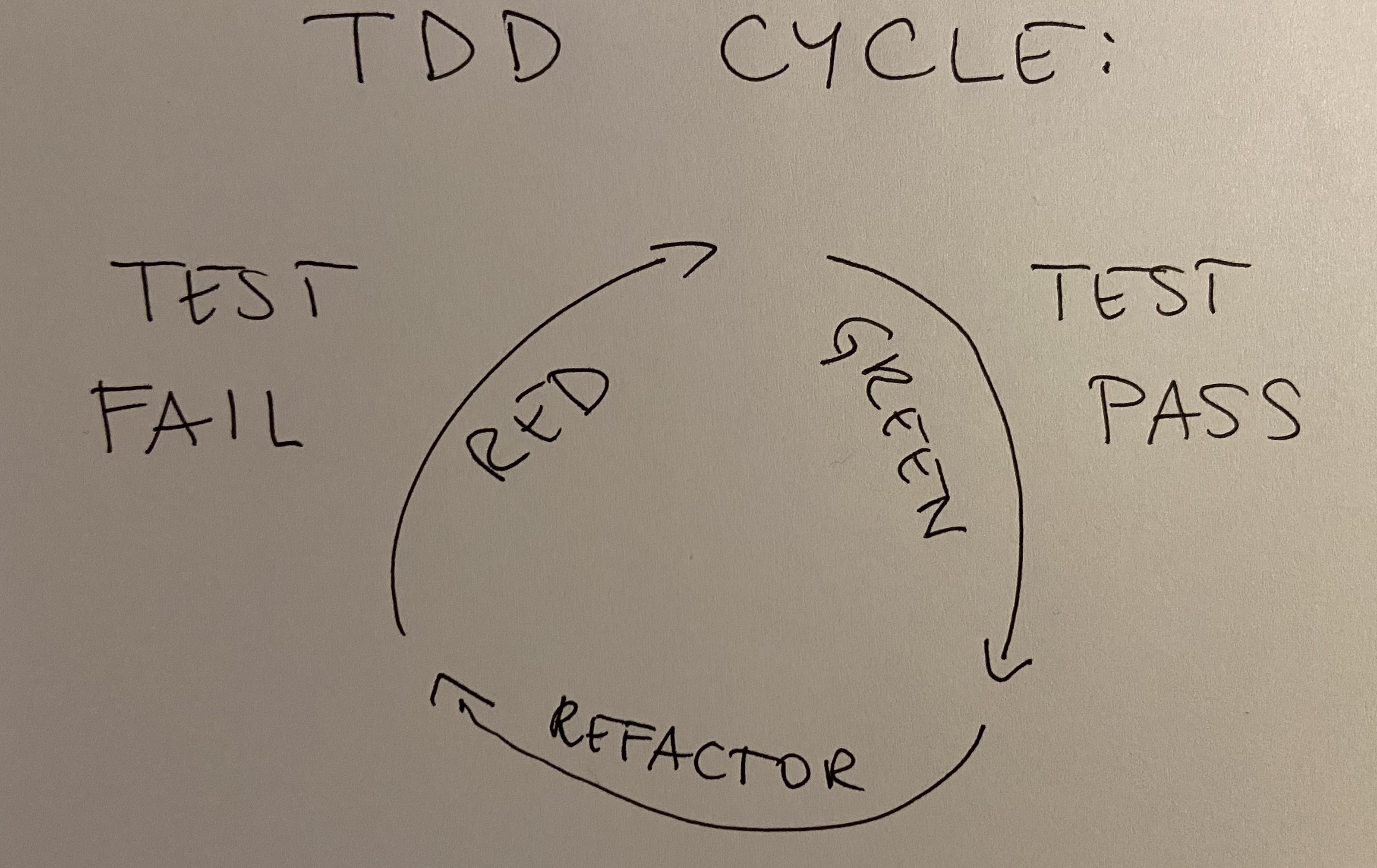
Well, I'm new to electronic engineering, but I'm no stranger to software development. What developers do to ensure their mission critical code runs correctly? They apply one of many proven techniques to ensure code correctness, and one of them is Test Driven Development where you start with writing tests that your software absolutely must pass. Your tests are not based on observations of the encountered or expected failures, your tests document the critical requirements. If your software must ensure safe plane landing you don't test altimeter reading, you test for collision, and first flight ends in flames :)
Basically, to consider TDD execution to be proper, you have to ensure to see the test fail the first time. If you wrote your code first and the test later - you are doing it wrong. If you wrote your test first, and then your code that works - you are doing it wrong. You have to see your test fail to know that the test itself works correctly. Only then, when the test finally passes you can consider the code correct.
So, how do we go about this approach with the problem at hand?
There is just one requirement here: clock cycle can't be shorter that half the maximum CPU frequency. So, if the maximum for modern 6502 is 14MHz, then neither of the clock phases can be shorter than 35ns (half of 71ns which is 1sec/14.000.000).
So, we need to generate special test fixture that will toggle clock selector in a way that ensures shorter than 35ns cycle. Then, we need to come up with a test that will catch these occurrences. And only then, when we prove we can see the test fail, we can go about finding a fix for the problem.
Initial setup of the test fixture
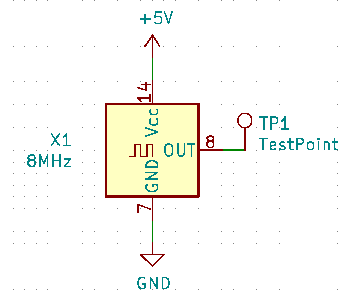
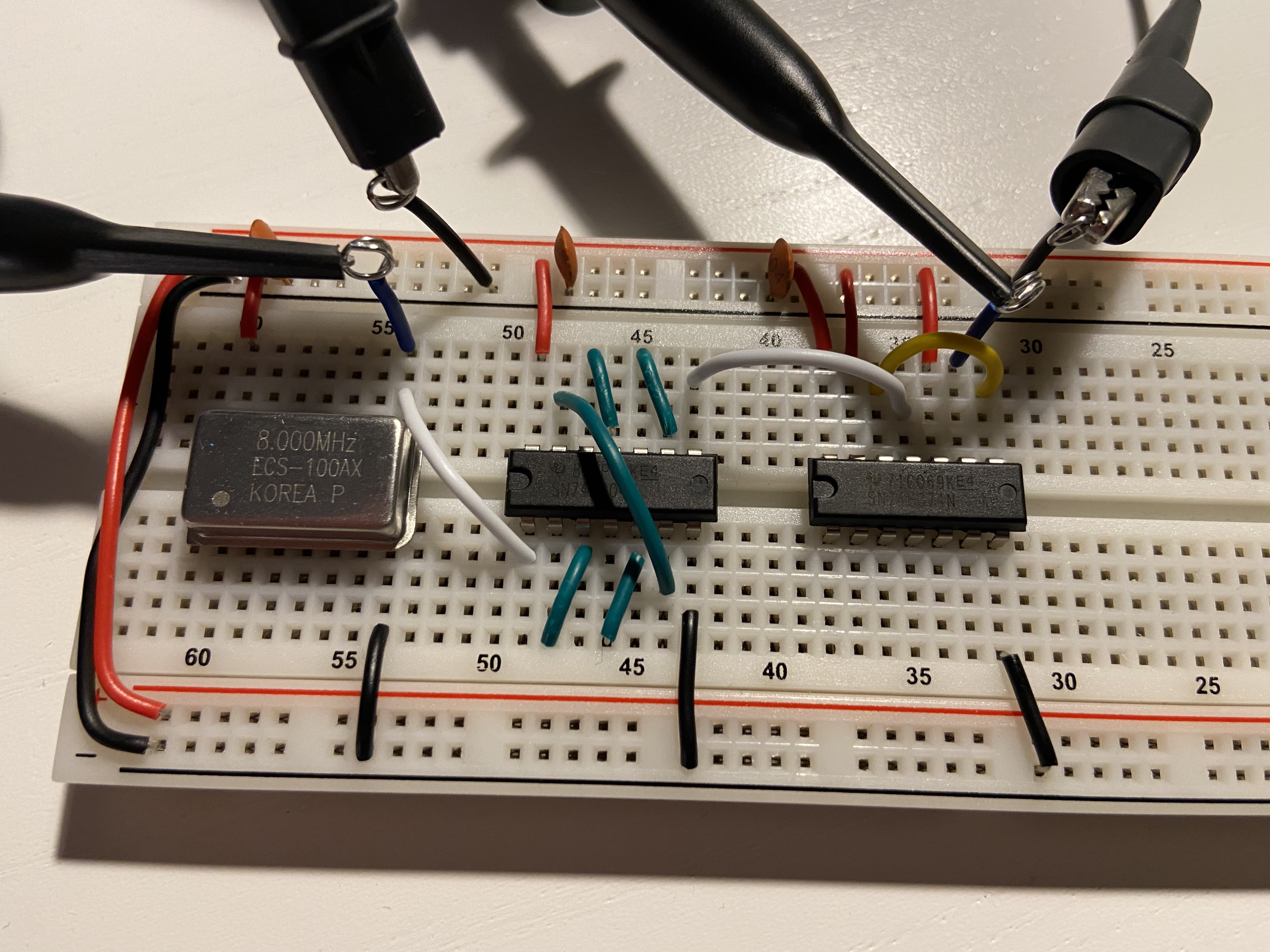
Let's start with the basics: we will need a clock, say 8MHz, that will generate the basic signal:
![]()
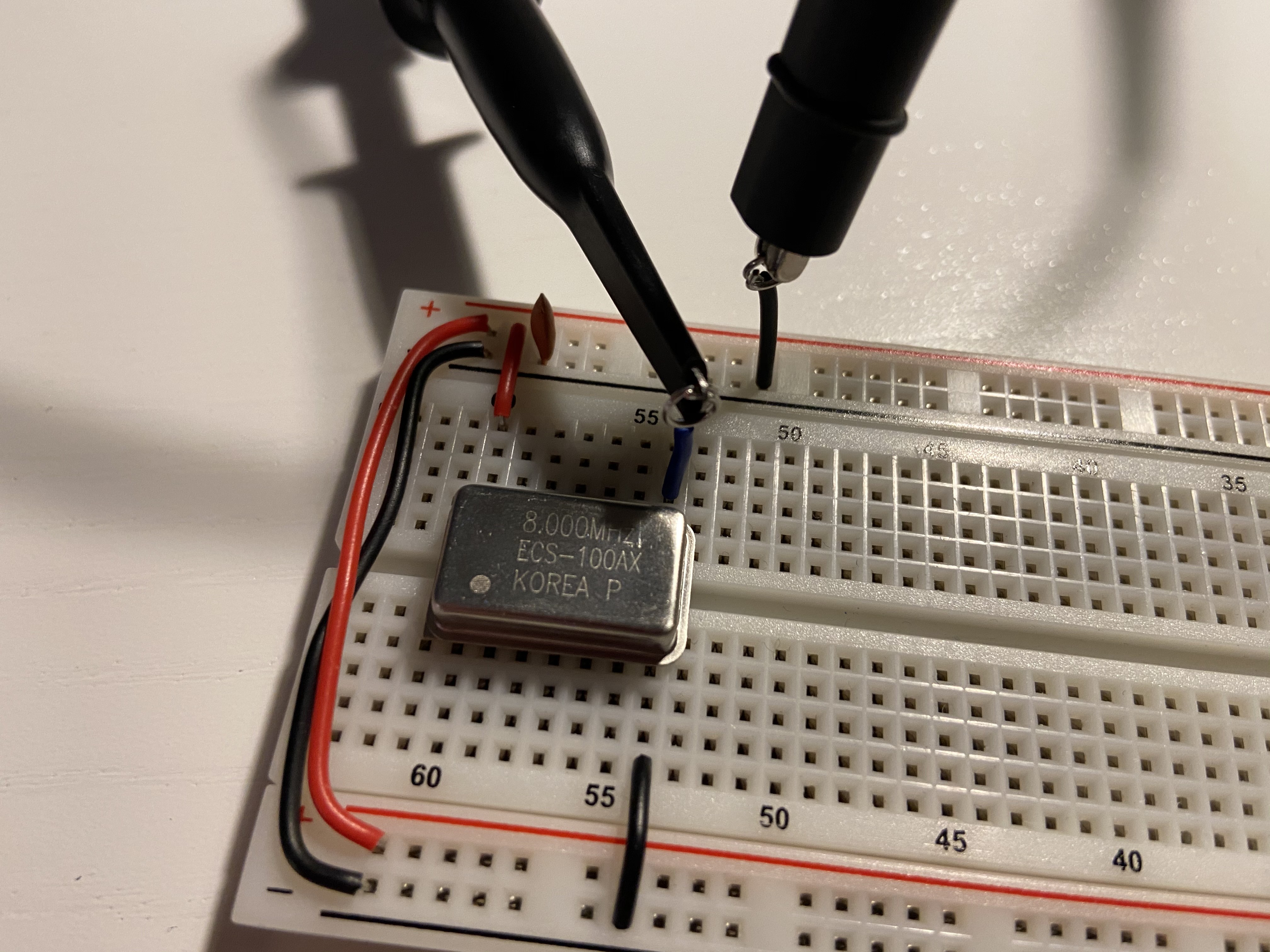
Build it on breadboard:
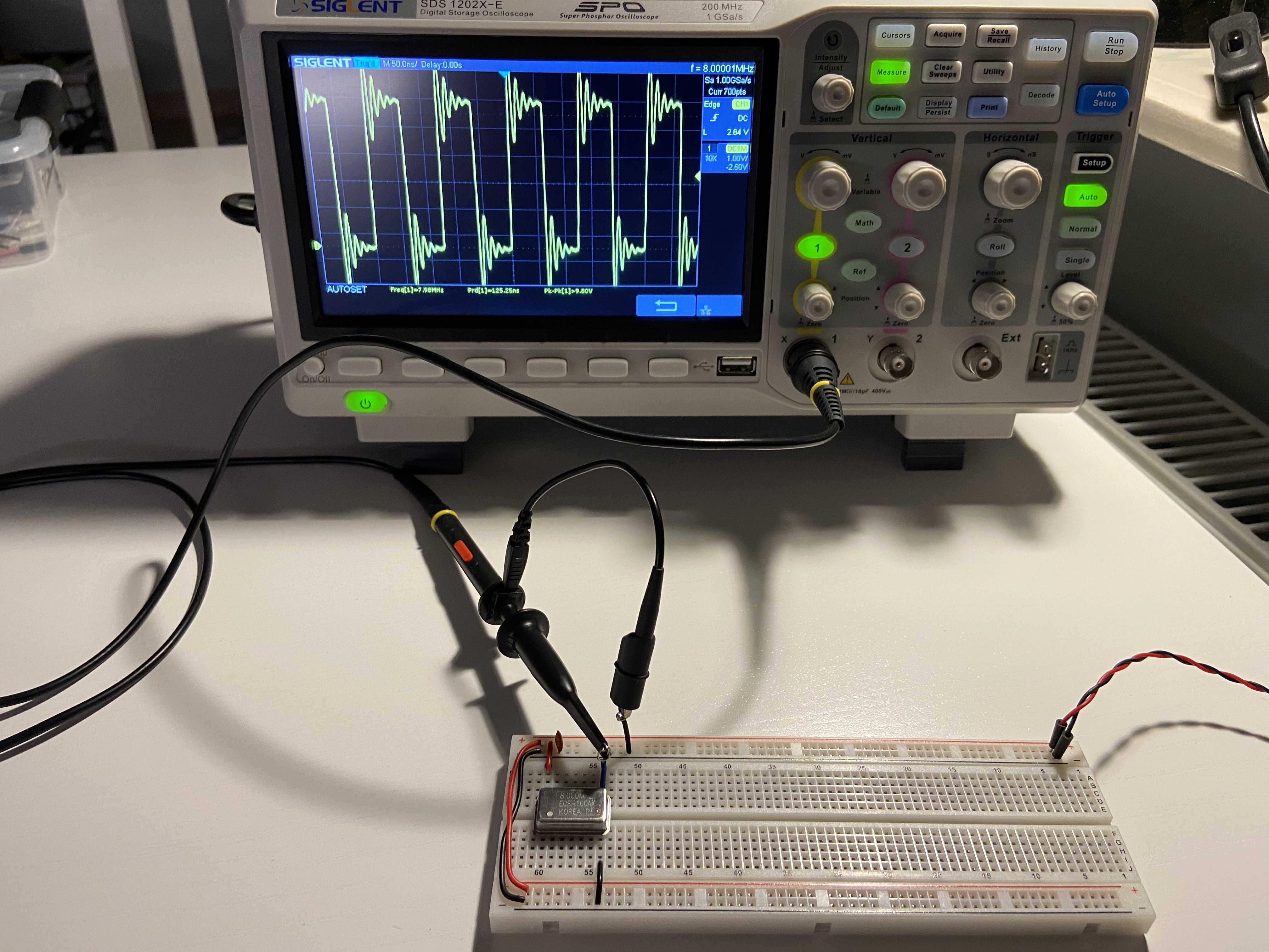
Measure to be sure:
Sorry, had to show my toy again :) Close-up:
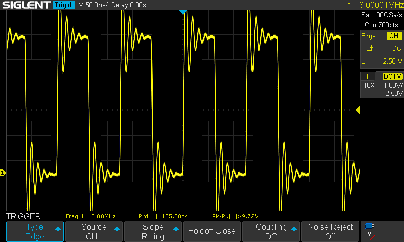
![]()
Nice, we have a clock. It's ringing like hell, because I'm too lazy to install all these springy things on my probes. Whatever :)
Add some delay to it
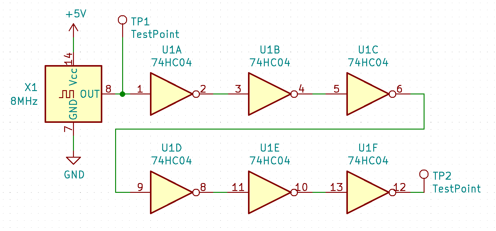
Now, the clock switch will have to happen shortly after the clock cycle has started. We can use hex inverter for it:
![]()
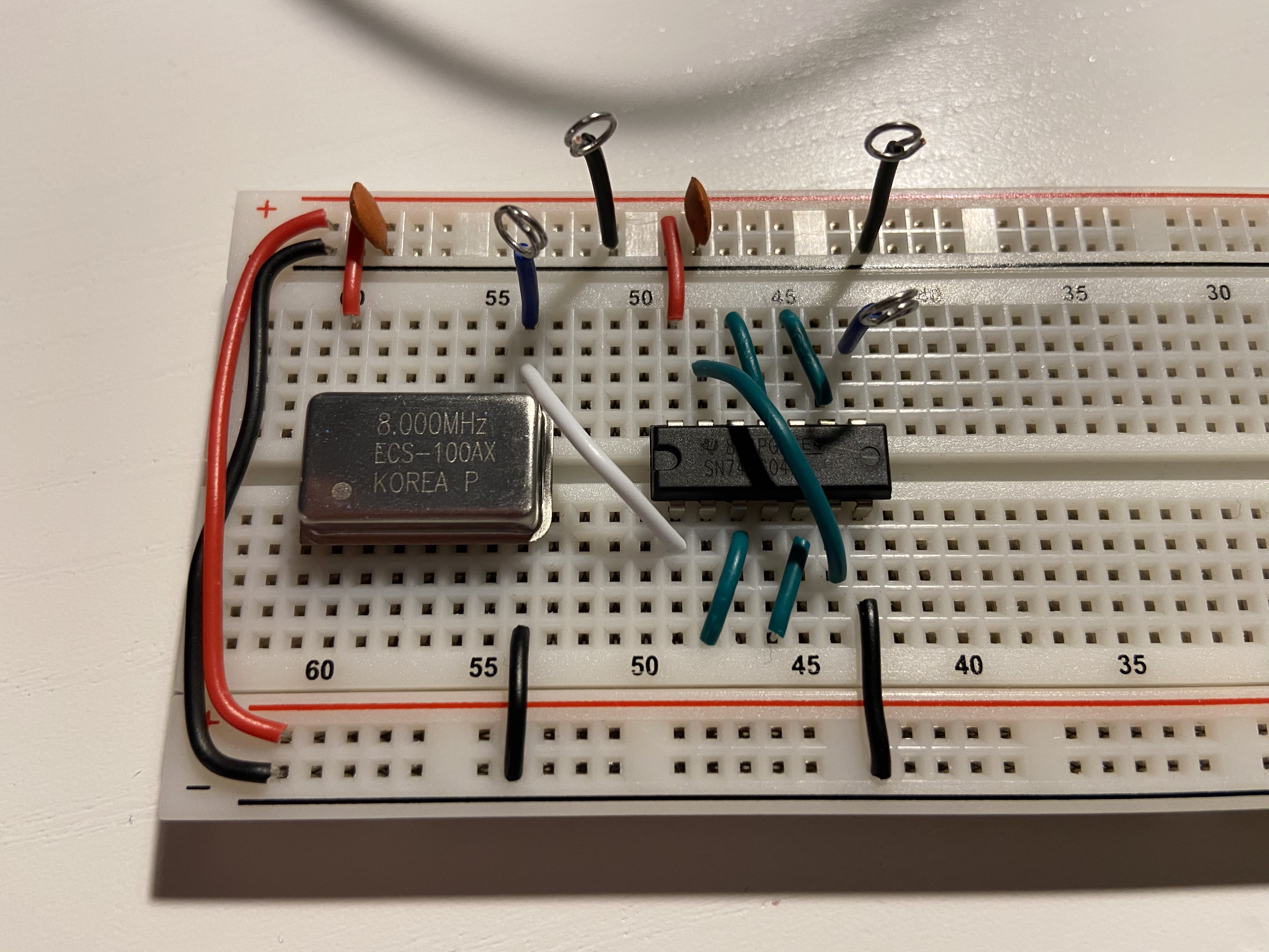
Each gate has some propagation delay to it, so when accumulated it should be pretty visible. Build on breadboard:
Measure to be sure:
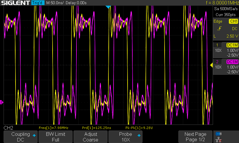
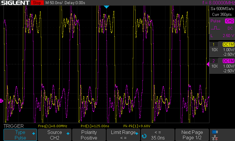
![]()
Great. We can see that the second test point registers noticeable delay.
Clock switching
Now, since we have the alternating signal delayed to the clock, we could move on to installing the mux now (and use the pink signal as clock source selector), but this would give us only single scenario, where clock toggle always happens at the beginning of high clock cycle. We need something more varied: short cycles at both ends of the cycle.
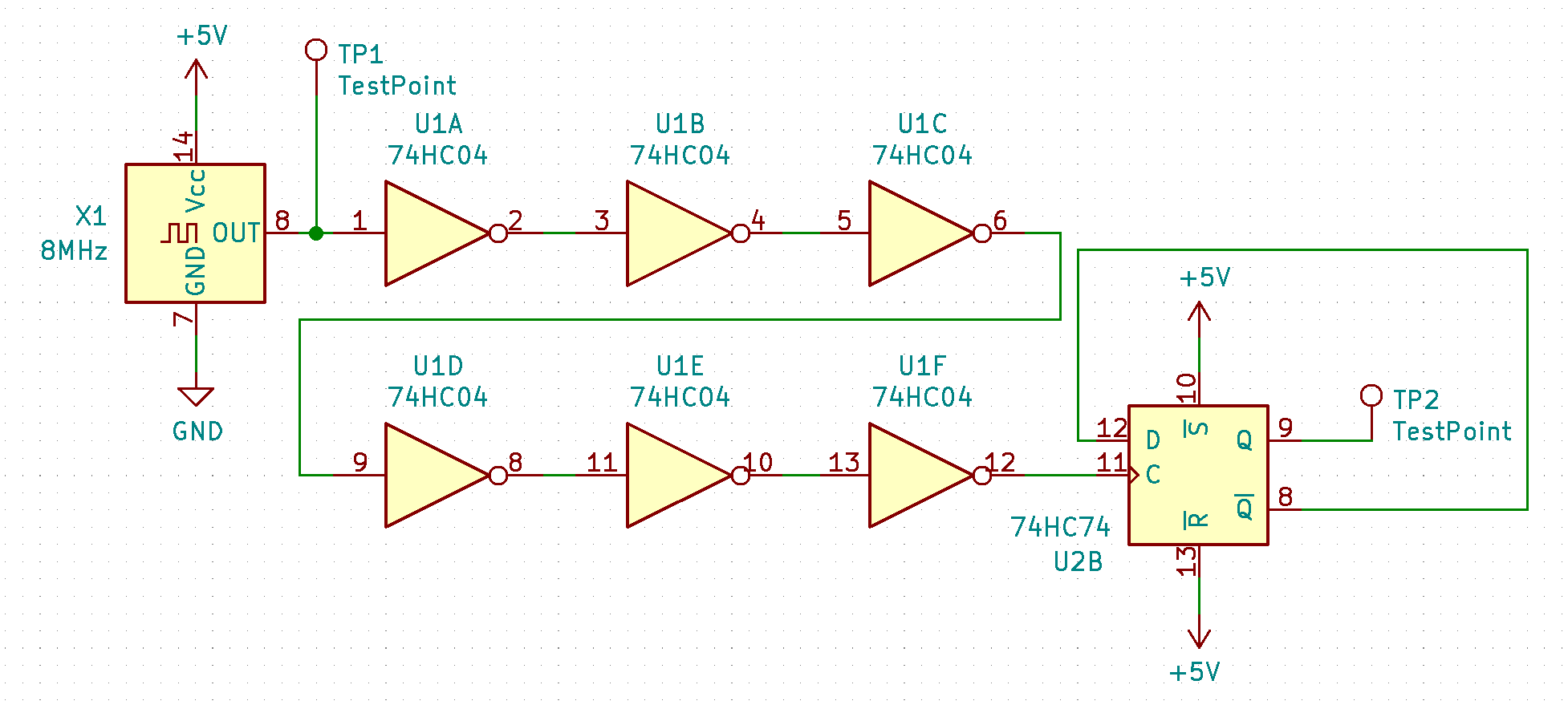
To do that, we will switch every other cycle: sometimes at the beginning, and sometimes at the end of high clock cycle. To do this, I will use D flip-flop that would basically produce clock switch signal every two main clock cycles:
![]()
As you can see, output of the flip-flop will always change shortly after the main clock rising signal, and it will alternate each time with the last state. This is how it looks on breadboard:
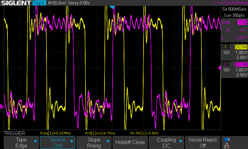
Now, when I measure the flip-flop output, I can see the following:
![]()
Now, let's assume that low output from the flip-flop (CH2, pink) selects main clock, while the high output selects AVR clock. Let's also assume that the AVR clock always starts low (we control its state programmatically, so we can always pull it low before the switch). Therefore I will build the mux circuit, but the AVR clock will always be low.
Looking at the diagram above you should be able to imagine how will the resulting signal look like: Wherever pink signal is high, the clock output will be low; in places where pink is low, it will copy the yellow signal. Resulting spikes will be much more narrow.
Adding the multiplexer
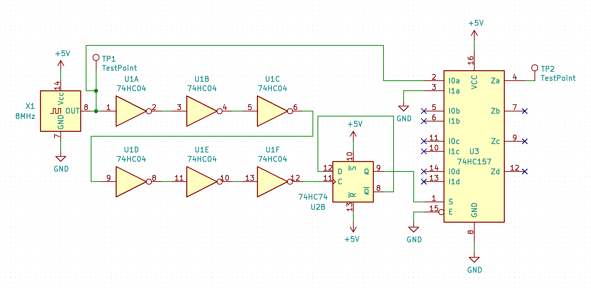
So, let's see if the hypothesis holds when we add the mux:
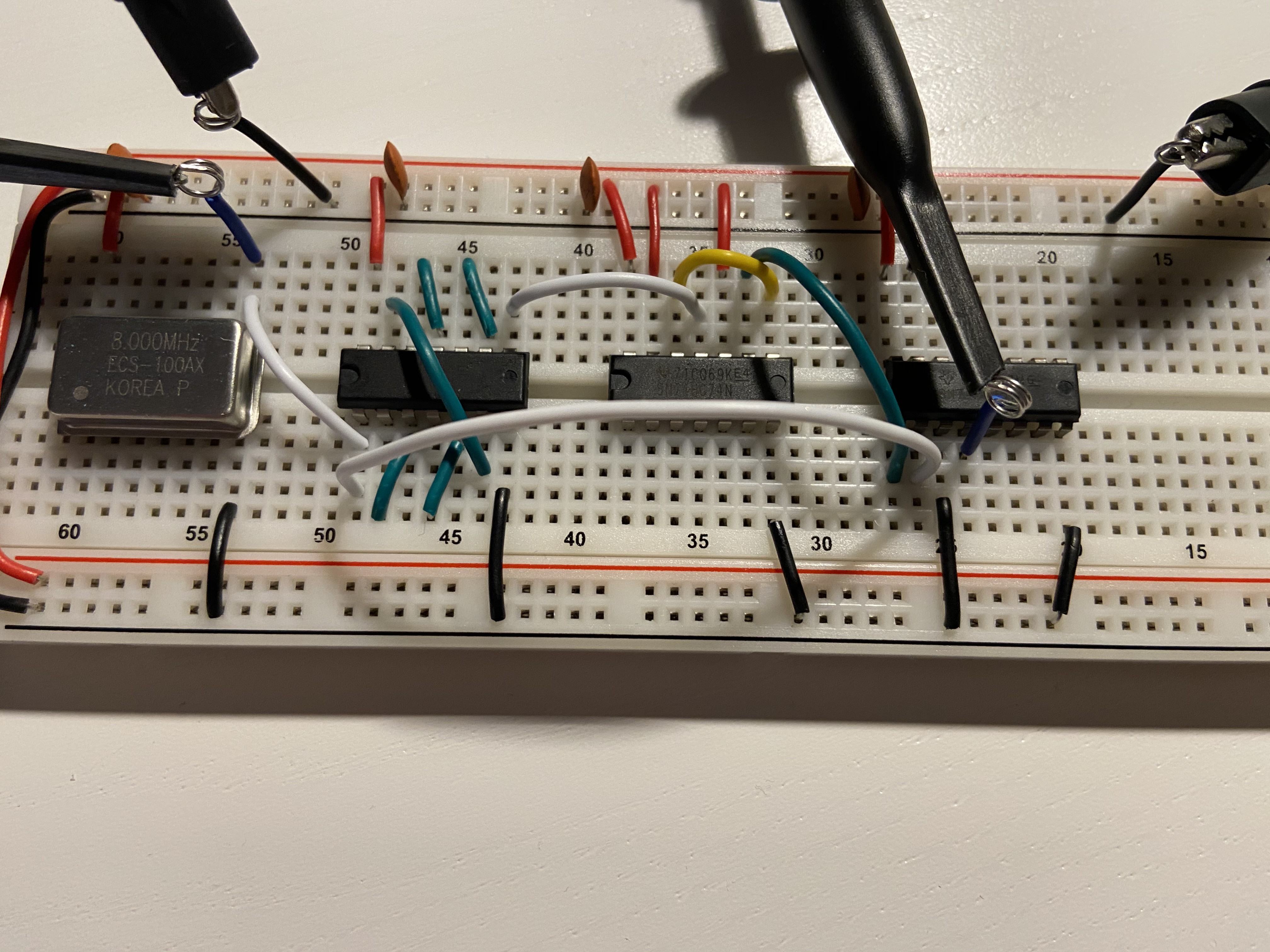
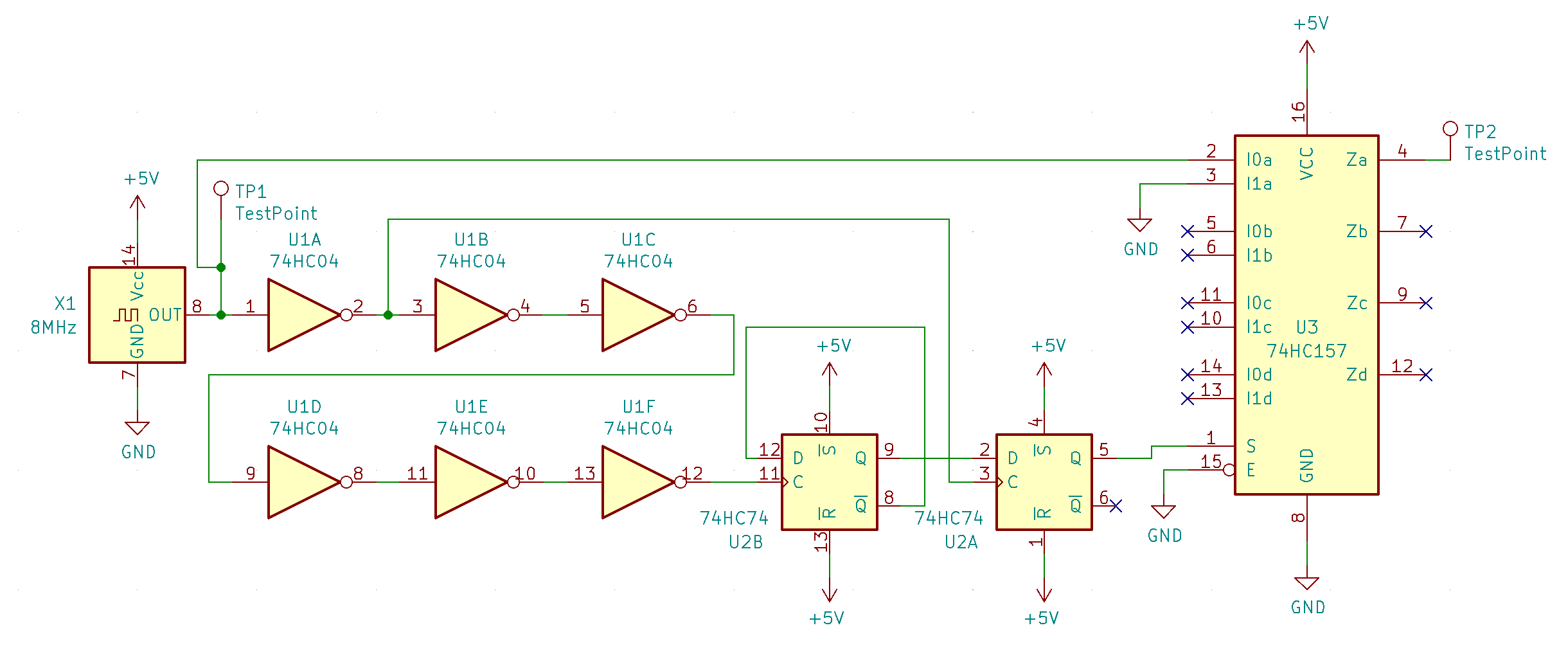
![]()
As you can see here, the output of flip-flop (pink signal on previous measurement) is driving select line of the mux. There are just two inputs: master clock on I0a, and permanent low on I1a as described above.
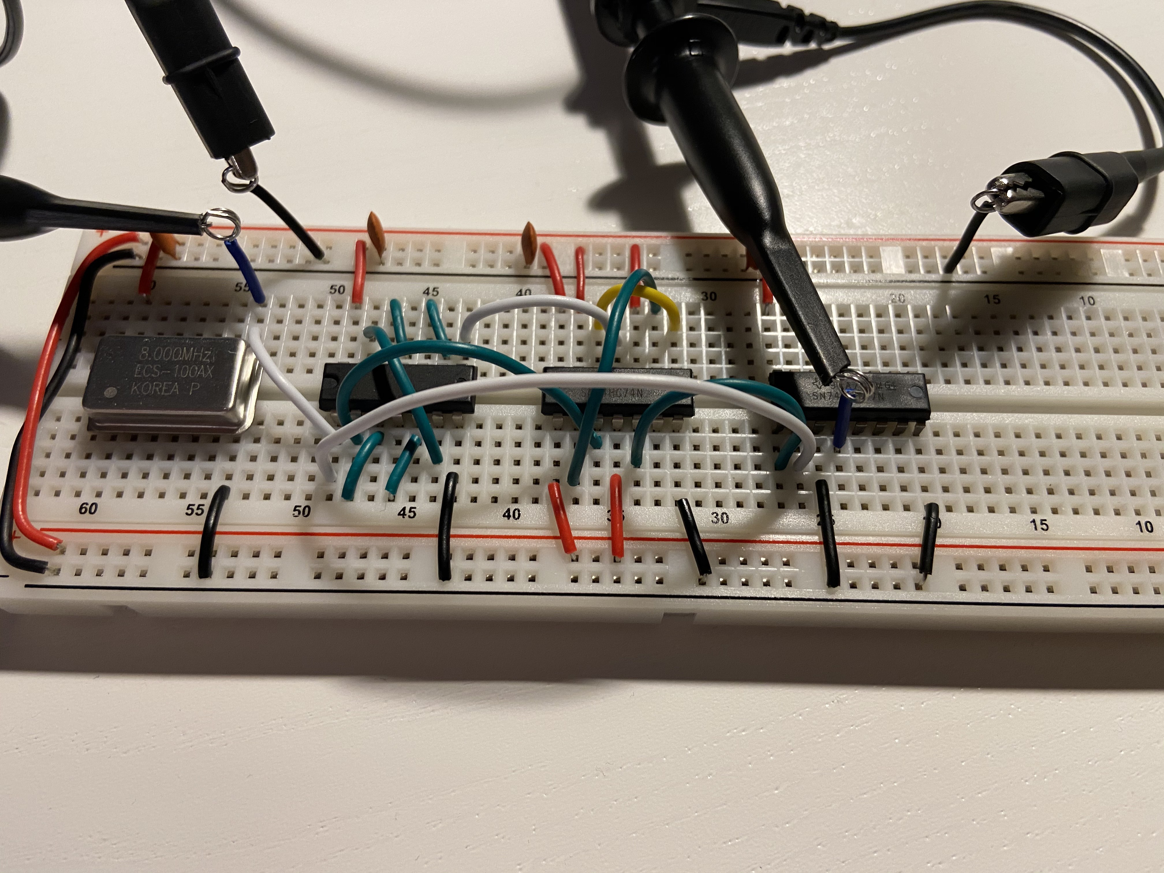
Breadboard build:
And now the fun part - the actual test case that should capture failure. We could run the oscilloscope and measure widths of the pulses to check them, and keep looking for ones that are below safe region.
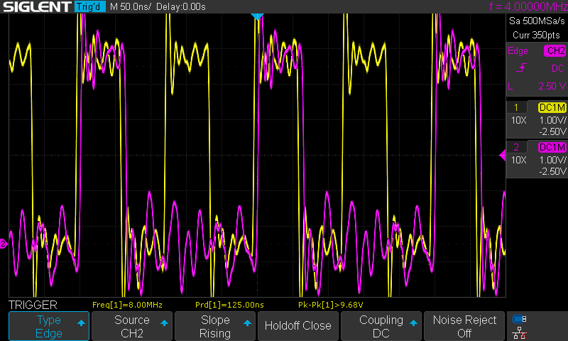
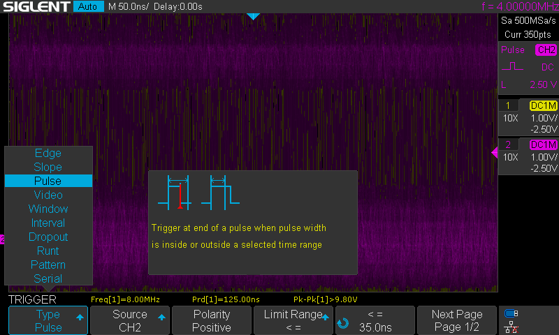
There is, however, better way to do it. We can set the trigger in the scope to look for clock pulses that would be shorter than 35ns:
![]()
This way it doesn't matter whether the pulse is happening every time (as here), or once every million cycles - scope will stop if it is found at least once. If it runs and runs without capturing the result, it means that there are no pulses that would cause CPU failure.
As you can see above, such pulse was found immediately, as per test design.
This is great - it means that we successfully built test fixture that produces signal that violates the CPU requirements. We are seeing red, yay!
Now we need to find a way to change the clock source selection circuit (that currently contains only the mux, the rest is really test fixture only) so that the issue doesn't occur anymore and our test passes each time.
Fixing the problem
Now, you probably know the solution to the problem already, and indeed it's pretty simple: we want to synchronise clock toggle operation with falling edge of the faster clock. There is very simple, standard way to do so. We just need to use the second flip-flop in the package:
![]()
This added flip-flop will "filter" any clock toggle request signal (produced on output of the first flip-flop), letting them pass only on the negative transition of clock. Please note: that the flip-flop clock is connected to inverted master clock signal. This implementation ensures that each clock toggle operation happens exactly at the beginning of clock cycle, when the clock is low. Hopefully, that is, but we are going to test it!
This is the breadboard build of it:
And this is how the clock signal looks on the scope:
![]()
As you can see, the clock toggle operation is synchronised with master clock, even with the clock selection signal specially produced to interfere with the solution.
In auto mode we can see that the scope can't sync to expected signal, which is already good sign:
![]()
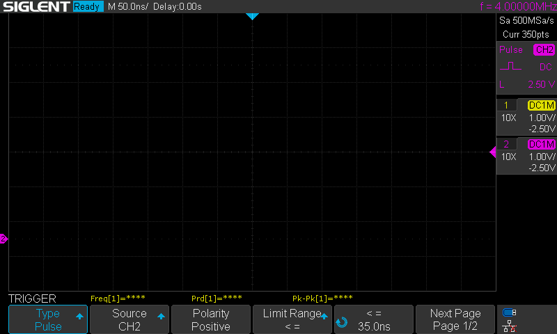
Let's try to capture single occurrence then:
![]()
Nope, none found.
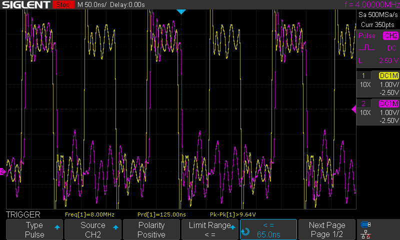
What if we increase clock pulse length?
![]()
Yeah, we do have a match. This means that our test fixture is working, our test procedure is correct and our solution to expected problem is working correctly. We have successfully completed full TDD cycle and have a solution that is proven to work as per initial requirements.
Let me know what you think in the comments below, please :)
EDIT: After having received comment on Reddit forum, I would like to add more information here. First of all, using single flip-flop can lead to serious issues caused by metastability. There is this Wikipedia article about the issue, but I find this explanation much better.
This means that to ensure correct clock operation, you should put the resulting clock selector signal through another flip-flop that will filter out any metastable output from the first one.
The other thing is related to synchronizing clock switch of two unrelated clock sources (case that is not really applicable to what I'm doing here), and there is very nice and clean solution for it described here.
As usual: the key takeaway is: share so that you can learn from others!
-
The curious case of reset button
10/16/2020 at 10:43 • 2 commentsUpdate on the DB6502 Proto Board
So, I've been playing with my DB6502 Proto Board for some time now, polishing the supervisor software recently, and it's pretty neat as it is now. You can flash ROM, you can obviously read its contents as well. You can run the 6502 using onboard AVR as clock source with speed ranging between 300KHz (system bus captured, no breakpoints yet) and 800KHz (system bus capture disabled). You can single step over single cycle or single instruction, so basic disassembler is already in place. Some screenshots:
![]()
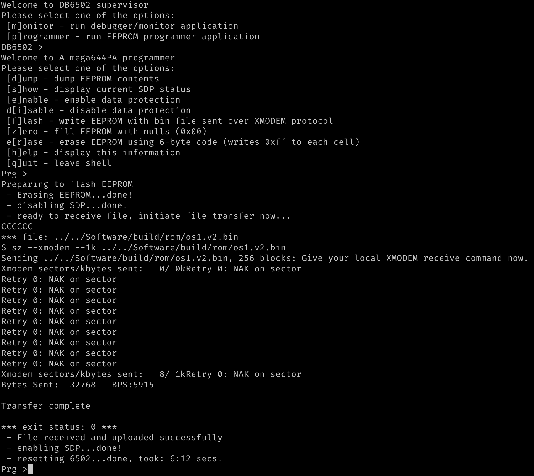
The one above shows how onboard AVR is used to flash OS/1 system image to EEPROM.
![]()
This one - dump EEPROM operation and entering monitor shell.
![]()
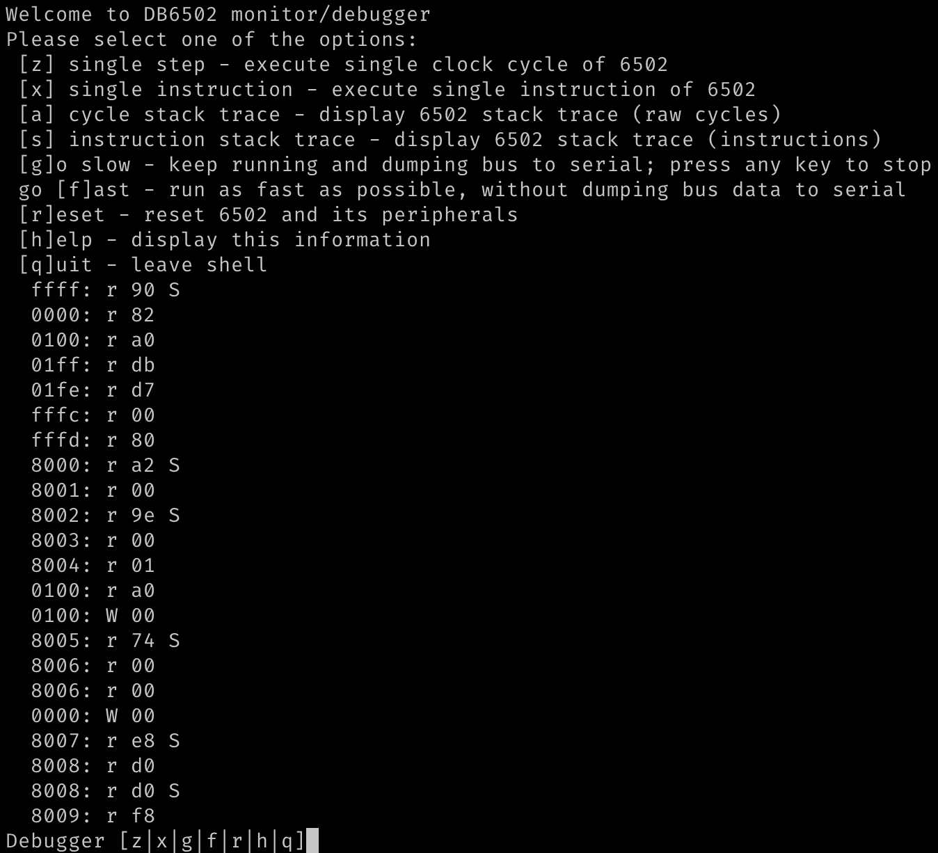
You can single-step the cycles...
![]()
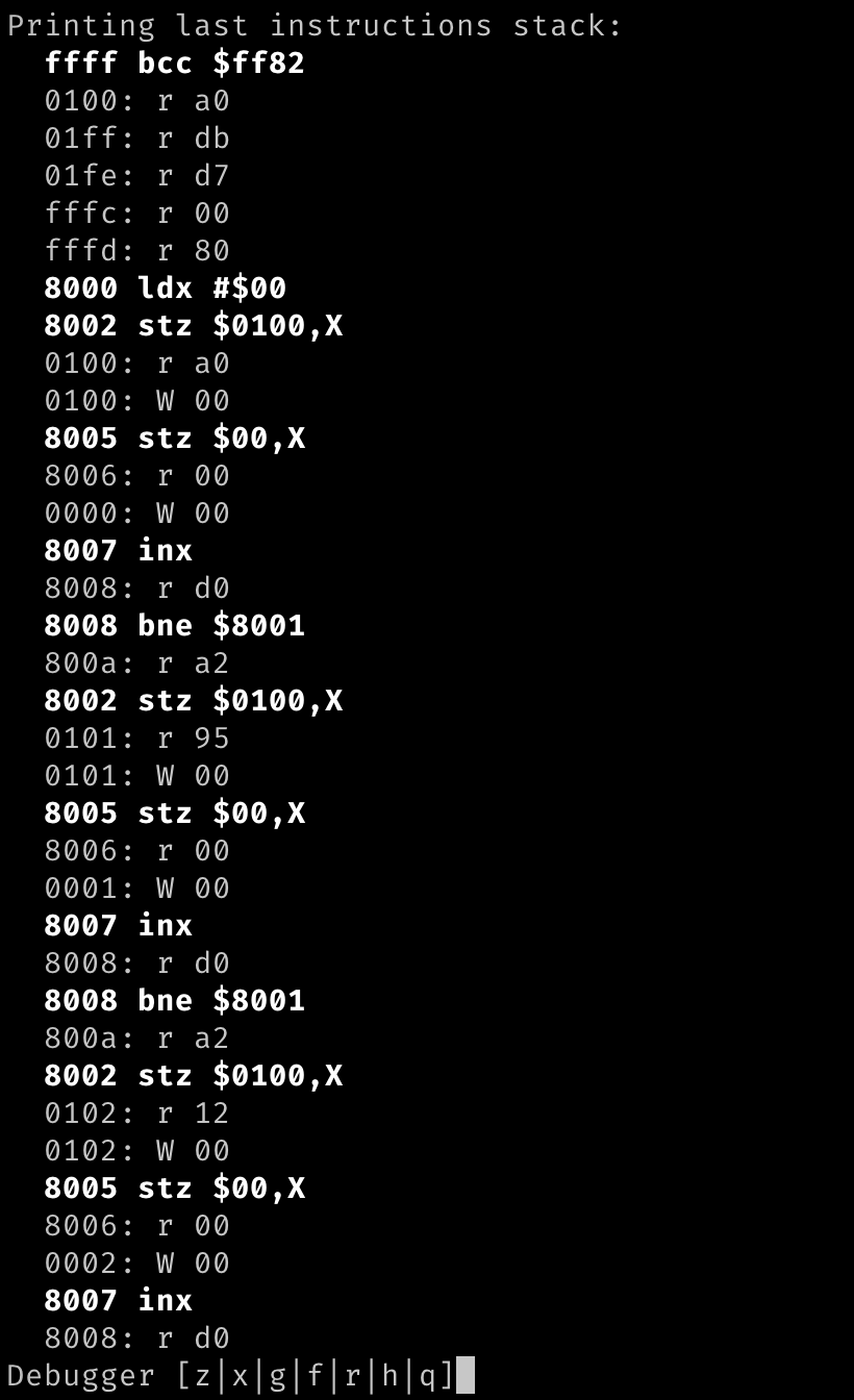
And whole instructions.
Finally, you can run fast to get enough performance to run OS/1 on the board:
![]()
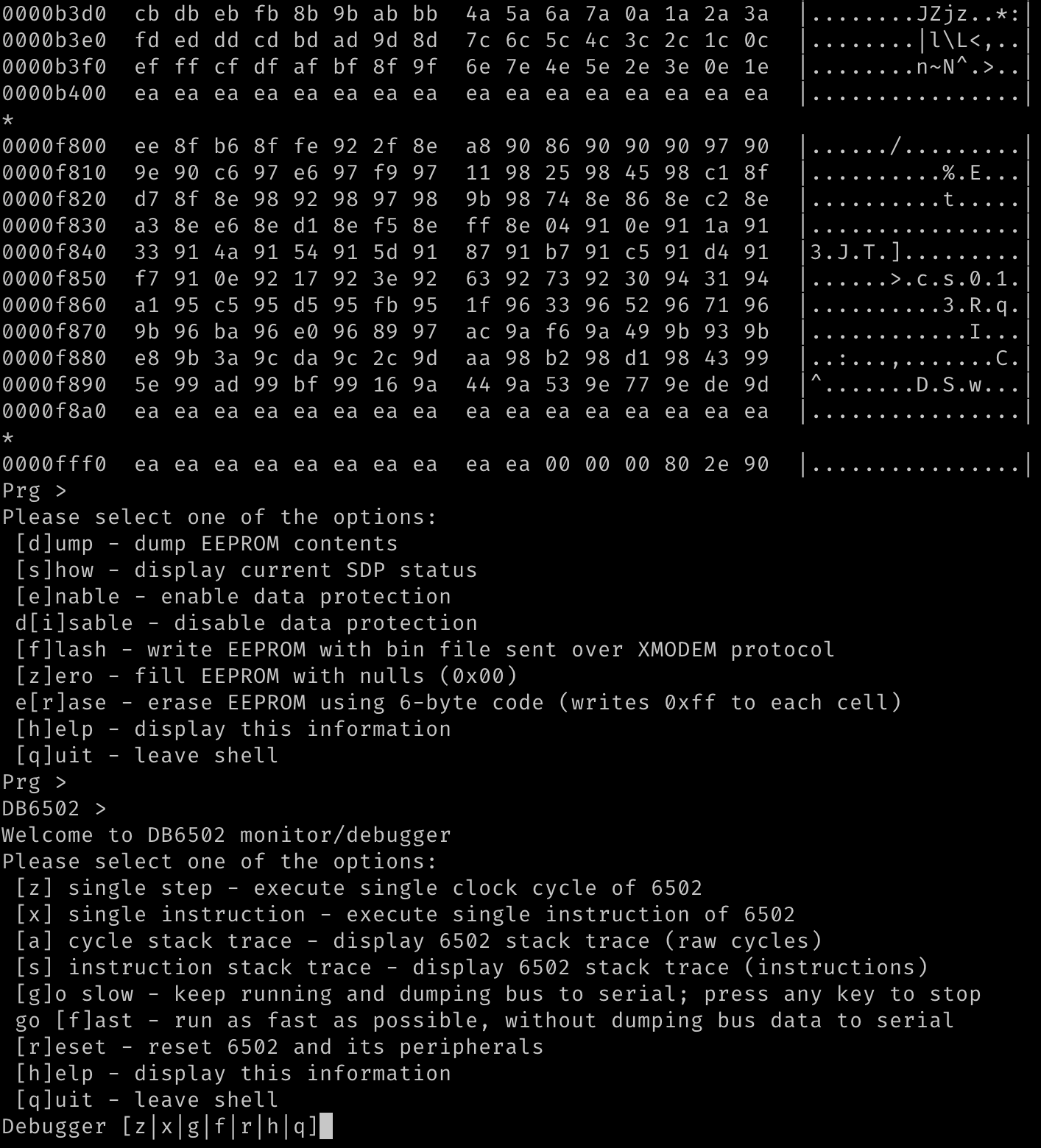
I have also implemented major redesign to OS/1 serial interface architecture, it's using replaceable (at compile time) serial driver modules, and I created one for my next-gen DUART controller, so it works with three different chips now.
So yeah, I've been busy recently, and it all worked pretty fine, with one simple exception.
Reset circuit explained
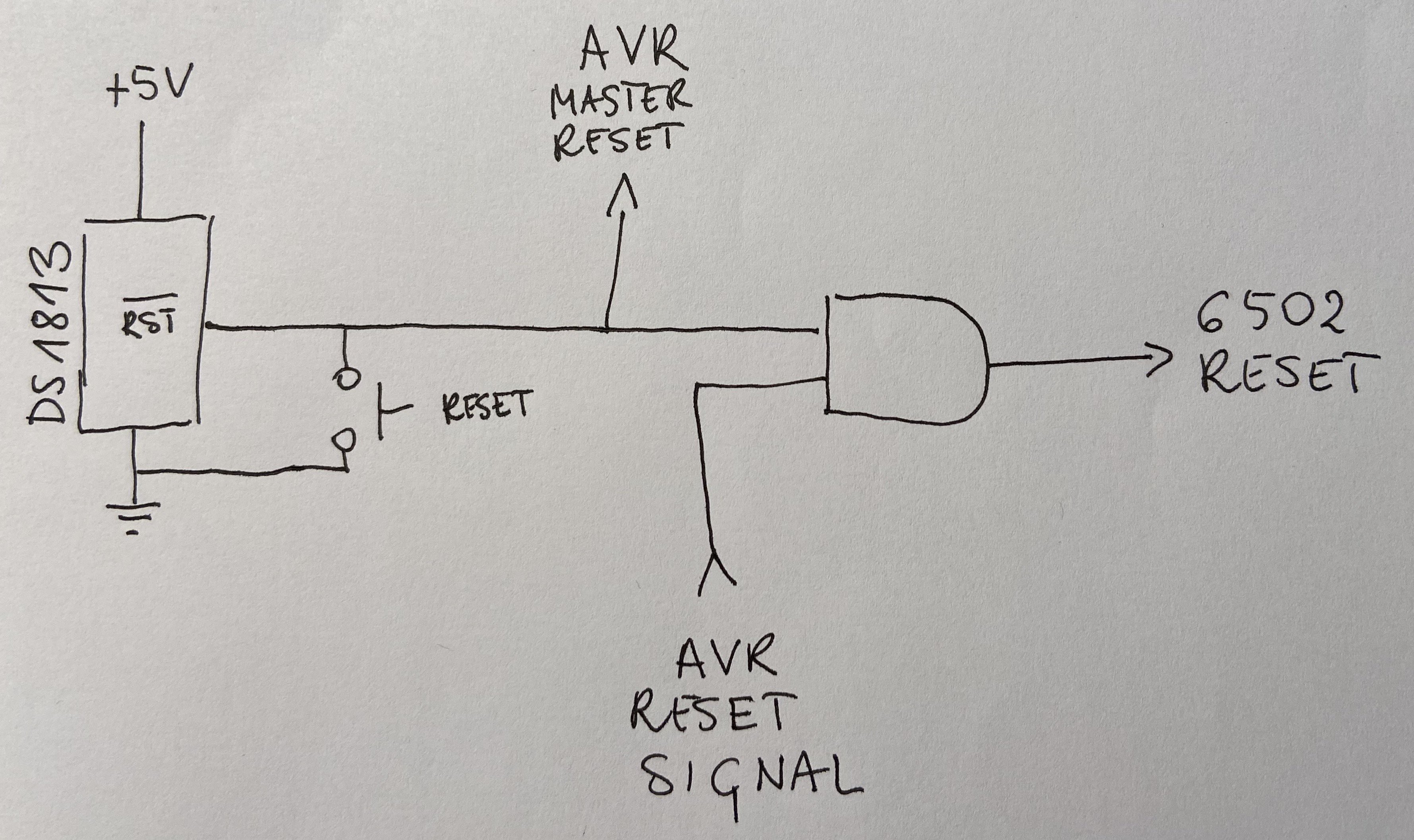
So, there are two reset circuits on the board, and the same design will be used in the final version. There is primary master reset circuit connected to DS1813 chip that resets everything on the board (with the exception of the UART->USB interfaces, see below). However, I wanted to have another, secondary circuit, used to reset only 6502 and its peripherals. The reason to do so is that you might want to use your AVR supervisor session over several 6502 resets. You want to keep your breakpoints for instance.
The solution is pretty simple: both reset signals are active-low, so the master reset is connected directly to DS1813 chip (that generates the signal on power-up and when reset button is pressed) and AVR and its peripherals. 6502, however, is connected to secondary circuit that is generated as an output of AND gate. The inputs are: master reset and signal originating from AVR.
This way we have two ways of resetting the 6502: by the master switch/power-on, or by command from AVR shell.
Now, this is pretty simple, right. Could anything possibly go wrong?
Well, I wouldn't be writing about it, if there wasn't.
The strange case of reset button
So, most of the time it worked, I could reset the 6502 from AVR shell and it would just work. Sometimes, without any apparent reason I had to invoke the reset operation more than once for it to kick in. That was weird, especially that my code for sending the reset signal was following WDC datasheet that requires at least two full clock cycles. I had three.
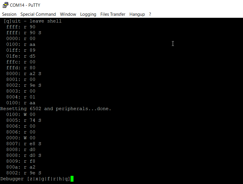
Still, sometimes what happened was this:
![]()
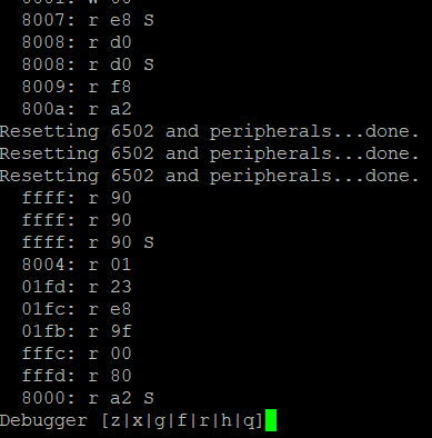
As you can see, reset sequence was performed, but the CPU continued as if nothing happened. In those cases I just had to repeat it couple of times to kick in:
![]()
I was ignoring the issue for a while, because it was just a small annoyance, but at certain point I decided to look closer at it. And what I found was eye-opening.
First investigation attempt
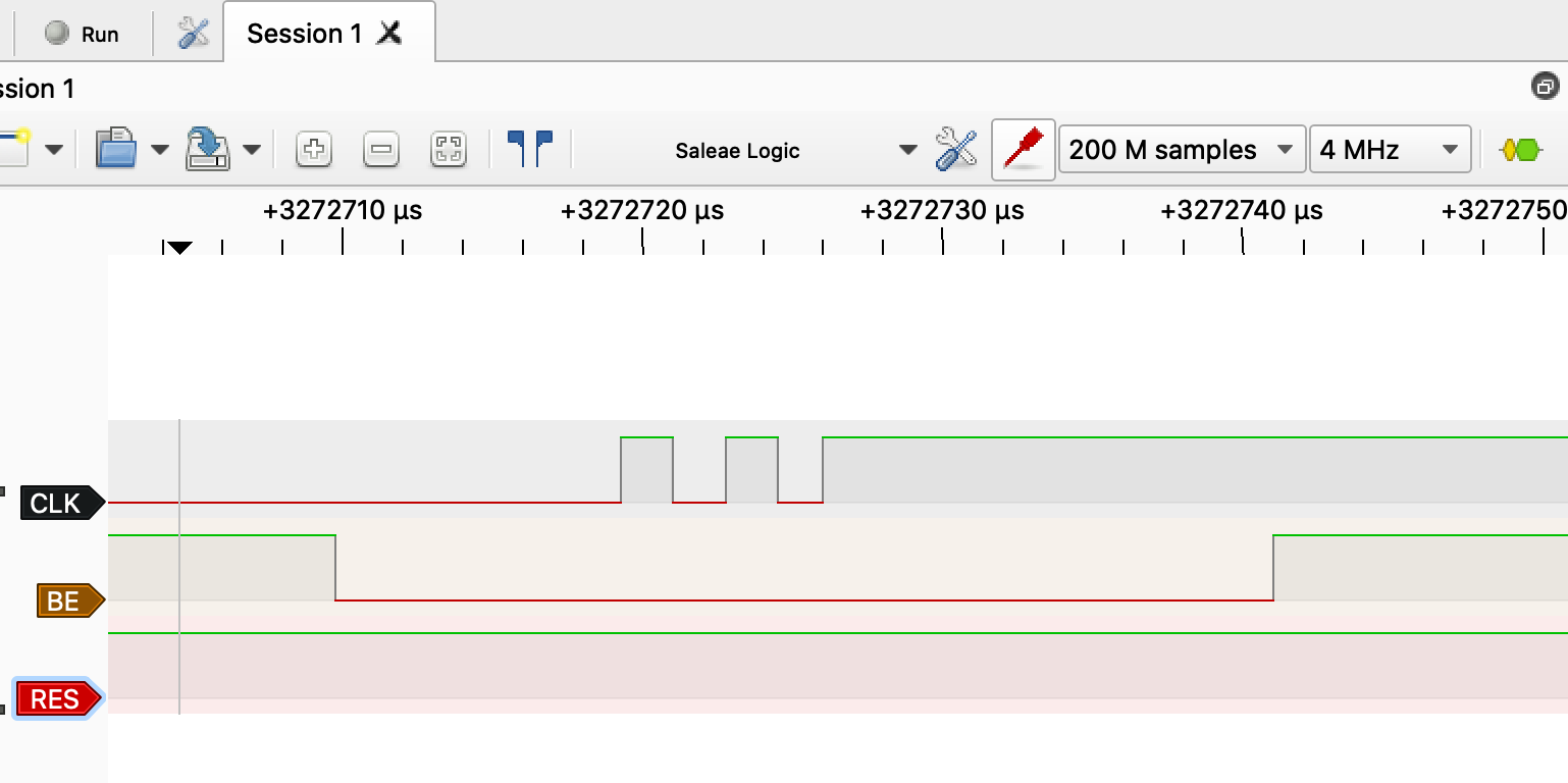
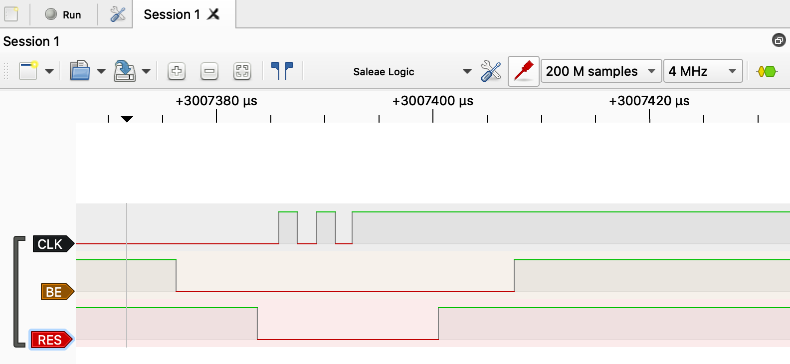
What do you do in cases like this? Get your logic analyser and see what it records. Here is what was captured using my cheap Saleae Logic 8 clone:
![]()
A-ha! Three cycles, bus taken over (it's not really necessary though for reset operation), but RES line was not pulled low. I checked the terminal, and the puzzle got all the weirder:
![]()
RES line was not pulled low, but the reset operation worked? WHAT THE HELL?
Probably the cheap clone is crap. Weird, but whatever. Let's get the serious stuff: 16 channels, 200MHz. Proper gear.
Second investigation attempt
What ensued was so strange I actually forgot to take screenshot of it, so what you will see below is my own recreation of the observed result. This is what I saw at much higher frequency logic analyser:
![]()
What got my attention here (but I wasn't able to replicate this afterwards), was the single high spike on RES line. It seemed as if the reset operation (triggered just after two cycles that WDC datasheet mentions) somehow drove the line high for very short period of time.
I was stunned. What is going on here?
Proper investigation attempt
I have to confess - I have finally gave in and got myself brand new shiny scope. Two channels, 1GSa/s, 200MHz Siglent 1202X-E. Oh, how I love my new toy! I got it couple of days after the observation of the above issue and decided it will be the first case I solve with my new gear.
Connected the probes, calibrated them, connected to circuit. Set up single acquisition mode, falling edge trigger on RES line around 1.66V. Connected the thing, run my computer and started trying to capture the signal.
Nothing.
Nothing.
Nothing.
Seriously, there must be something really wrong. I was about to cry, my new toy doesn't work, my reset line misbehaves, by logic analysers can't see the proper signal.
Changed trigger level to 3V and BOOM:
![]()
Yellow line is the clock input, pink is the reset signal. Can you guess what happened here?
It's always the wiring...
I have written this more times on Ben Eater's forum on reddit than I care to remember. Every week there is at least one thread about something not working (or working erratically) and the authors are always convinced it can't be wiring. It can't be error in wiring, because it sometimes/partially/almost always works.
And guess what: it always is wiring.
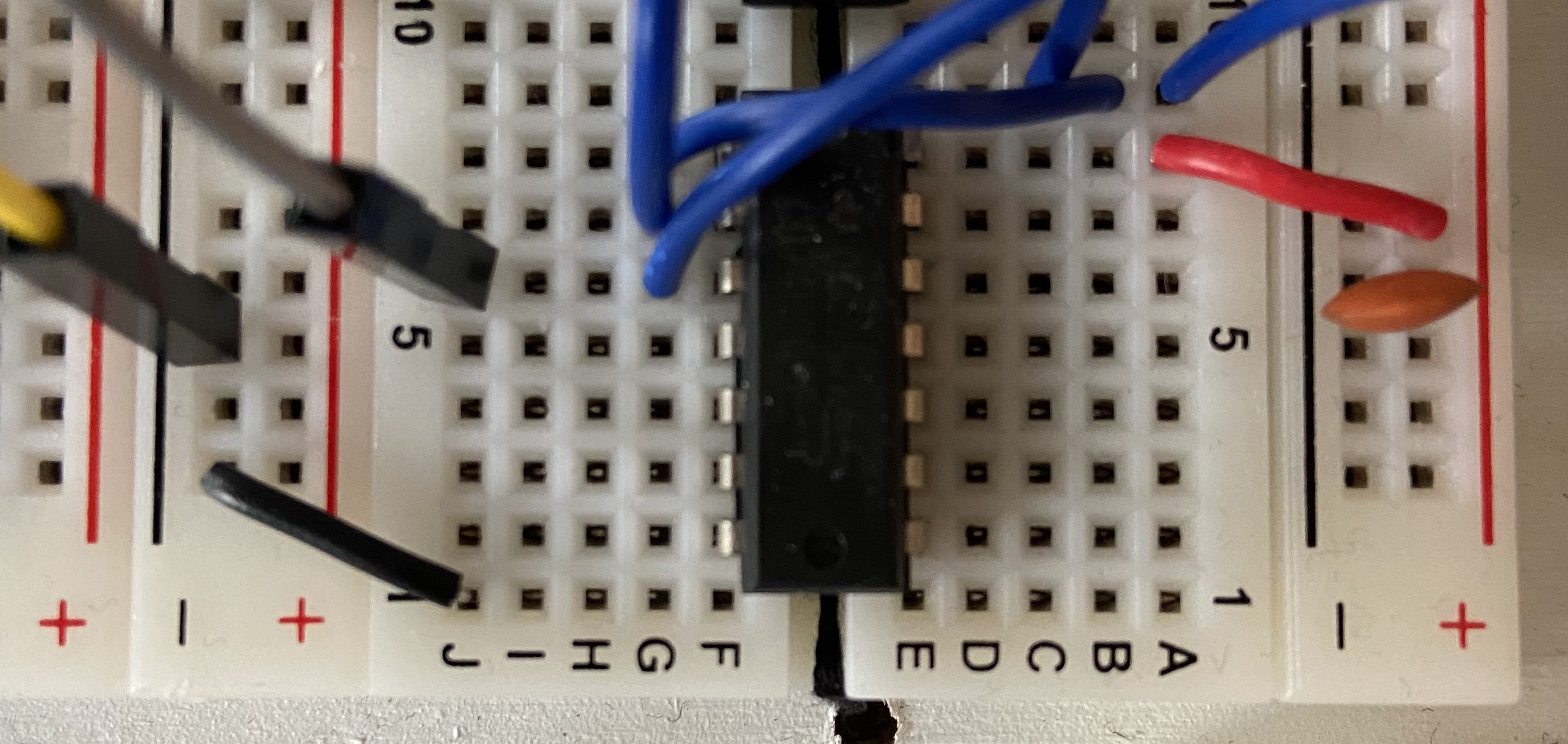
This particular case: wiring. Obviously. Check this out - wiring of the AND gate connected to reset line:
Yes, you are seeing it correctly. Yes, I didn't notice that for over three weeks staring at it every day. I missed it three times when connecting both logic analysers and scope probes.
Wire that is supposed to be connected to GND line on the AND gate chip (pin 7) is off by one breadboard slot, and the chip is not connected to any GND whatsoever.
Correction and test results
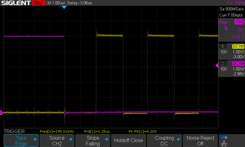
Obviously, when I connected the wire properly, this is what I see on the scope:
![]()
Also, my cheap and dumb logic analyser apparently it's not as dumb as its owner after all:
![]()
That being said, there are some key takeaway points here:
- Your system might work even with very serious design/execution errors,
- Small glitches are never irrelevant, they are very, very important clues that something bigger might be off,
- Cheap logic analyser actually seemed to work better than the expensive one,
- It always is your wiring. Ok, maybe almost always, but still: check your wiring again!
So yeah, it was another great lesson for me. I hope you enjoyed the read and learned a bit yourself too :)
-
Yet another story about "insignificant" details
10/08/2020 at 18:51 • 5 commentsLearning product development the hard way
One of the least expected consequences of sharing is that people actually take what you shared and start using it. To make things worse, these people are different than you, have diverse backgrounds, experiences and competences; they also use your design in a ways you have not imagined.
This, at least in my rather short experience, is the best part of the whole project. Every now and then I get messages from people all over the world who built DB6502 and ran into smaller or bigger issues while doing that. These issues let me see things from different perspective and are the best course in product design I could ever dream of.
At the same time this is the hard way, as you have to think of all the possible issues as much in advance as you can; negligence or ignorance can get you in trouble and while everyone seems to agree that authors of open sourced projects should not be held responsible for any consequences of their usage, you still will feel that you should address most of the comments you get in one way or another. So, prepare for bumpy ride and enjoy every single moment of the experience!
Think about target audience
This is something we all should know - consider the background of the people who will follow your project, and make sure you don't assume certain level of expertise. And yes, while you can expect at least some of them to be similar to you (after all, all great minds work alike), you have to ask yourself if you provide enough details for users outside of your demographics, whatever they might be.
One instance of such omission from my side was the unwritten assumption that most users of my project will have background in software development. After all, if you host your sources on GitHub and write documentation about compilation flags, you should expect anybody interested to be familiar with these things, right?
Well, wrong actually. Your project might be also followed by people who have never used git, so it's common courtesy to describe how to use it for the purpose of your project. You never know who's on the other side!
Key takeaway here: be careful with your assumptions, especially regarding your core competences. Remember how you got into electronics first and was upset about certain things never being explained clearly? This is exactly what happens to non-developers if you tell them to fetch the latest version of repo and switch to specific branch :)
The curious case of blink LED
One of the features I put on my DB6502 board was simple LED driven by remaining line on port B (other 7 lines are used to drive LCD screen). The schematic is as simple as it can possibly get:
![]()
Few weeks ago I was contacted by one user, let's call him Adam, who started building DB6502 and while very competent in electrical engineering, he was struggling with the software development toolkit that I used for my software. He managed to use VASM to create simple ROMs to run on the board, but was unable to follow the instructions for building my code.
I have to admit I put quite an effort to ensure that my software builds "out of the box" on each of the major operating systems (Windows/MacOS/Linux), but the documentation of the environment setup was lacking in that regard.
So, I started exchanging e-mails with Adam, guiding him step by step of the process.
To be fair - I have already done similar things in the past, improving my documentation with comments coming from other people, but it was first time that non-developer started working with my project. I expected this one to be pretty quick - five to ten e-mails maybe, simple suggestions and done. It turned out to be more complicated and it taught me a lot!
After we got to the point where ROM images would compile nicely, it seemed as if it would take just a few more steps to get to working OS/1 image. Unfortunately, this was not that easy. When we got to setting up the serial connection, weird things started happening. Transmit would work, but receive would fail. OS/1 image would not even boot properly. So many things seemed to fail it was a bit overwhelming - and to be fair, it's not easy to debug someone else's build with 11 hours timezone difference.
Significance of "insignificant"
One of the things that happened over the course of investigation was that Adam told me that the Blink LED is constantly lit. While weird (it should not happen, come on, too simple to fail), it didn't seem as something that needed attention. Short maybe?
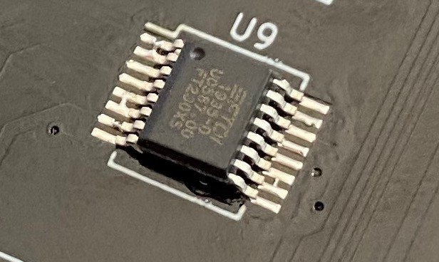
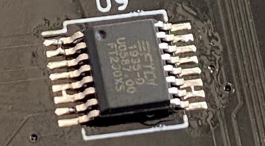
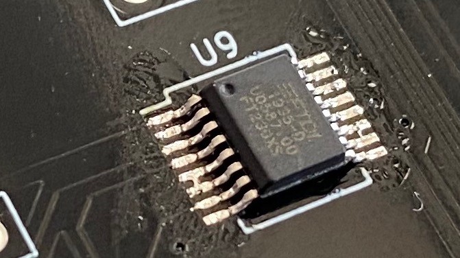
We focused on the more pressing issues with the transmit/receive operation on serial port. I was afraid it might have been caused by incorrect soldering of the FT230XS chip - it's the single most difficult part of the build and many people reported problems with it.
That being said, Adam was experienced engineer, people like him don't make such mistakes, and he didn't either.
I created several ROMs just to test his build. Programs as simple as they get to use different features of WDC65C51 (serial chip used by Adam) just to see where the problem might be. Pretty soon it turned out that synchronous communication (not using interrupts) worked just fine.
You are probably thinking "ah, the infamous WDC IRQ bug!". Nope, not this one :)
Being fully aware of the bug, I created the async version of the code using only the receive interrupt (transmit was still done in synchronous way), and it worked perfectly on my own board.
Yet, Adam's build didn't seem to work with it correctly. It would indicate (using other LEDs) that receive operation worked, but there was no transmit. As if the incoming data would not trigger receive interrupt?
After hours of looking at the schematic I started thinking that maybe the IRQ happens, but due to simple mistake Adam replaced 4K7 pull-up on the IRQ line by the adjacent 27Ohm resistor used for USB connection. This kind of strong pull-up might be too strong maybe?
Nope, this was not that again.
What was it then?
Adam spent several hours troubleshooting this and noticed interesting thing: the IRQ line of WDC65C51 was actually being correctly pulled low after incoming byte, but CPU seemed to ignore it. Further inspection revealed the reason: both VIA chips were pulling their IRQ lines low all the time. He added pull-up resistors to their IRQ output lines and things started working.
Then again: why did he need to add these pull-ups? I mean: nobody has ever needed them.
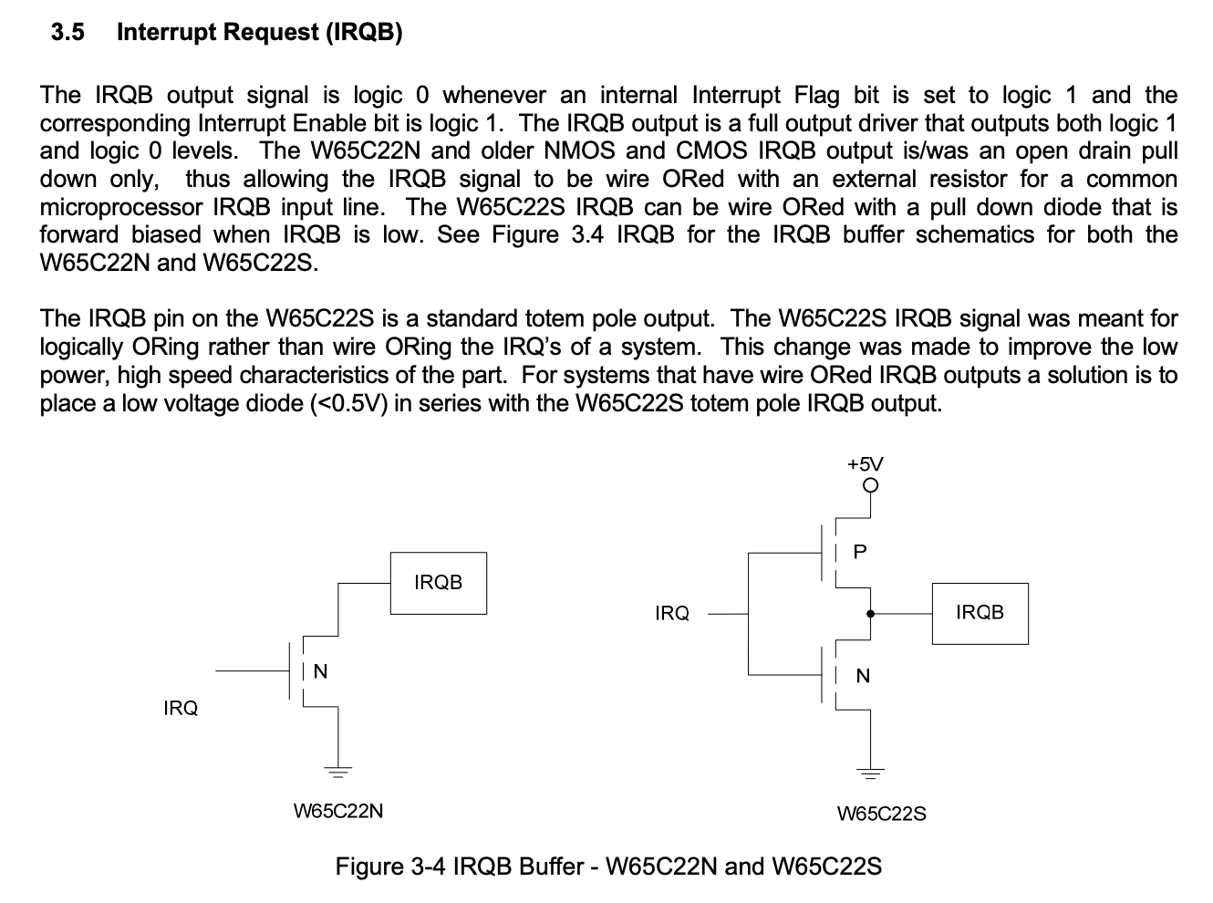
Adam found the answer. There are actually two variants of WDC65C22 chips: WDC65C22N and WDC65C22S. What's the difference? Glad you asked. If you check the datasheet, you will notice that there is important difference in how these chips handle IRQ line output:
![]()
So, as you can see, there is fundamental difference as to how these two chips work.
VIA was constantly pulling the IRQ line low (by simply floating), resulting in constant LOW on CPU input. As a result, CPU was executing only the IRQ handler code, and each time it exited IRQ handler, it would jump straight in. This is why it never could transmit any data - remember that WDC65C51 code for sending data can't use interrupts because of the bug.
Why did the other things work?
This was another riddle. How comes the CPU worked fine with all the other ROMs? I mean being stuck in an endless IRQ handling loop doesn't seem like something that would go unnoticed, right?
Took me a while to figure it out, and it's pretty obvious when I finally did: 6502 boots into mode with IRQ handling disabled. You need to enable interrupts by invoking CLI opcode. All the other programs didn't use interrupts, and since the point was to make them minimal, there was no CLI opcode in them. Mystery solved :)
So, what does this have to do with the Blink LED?
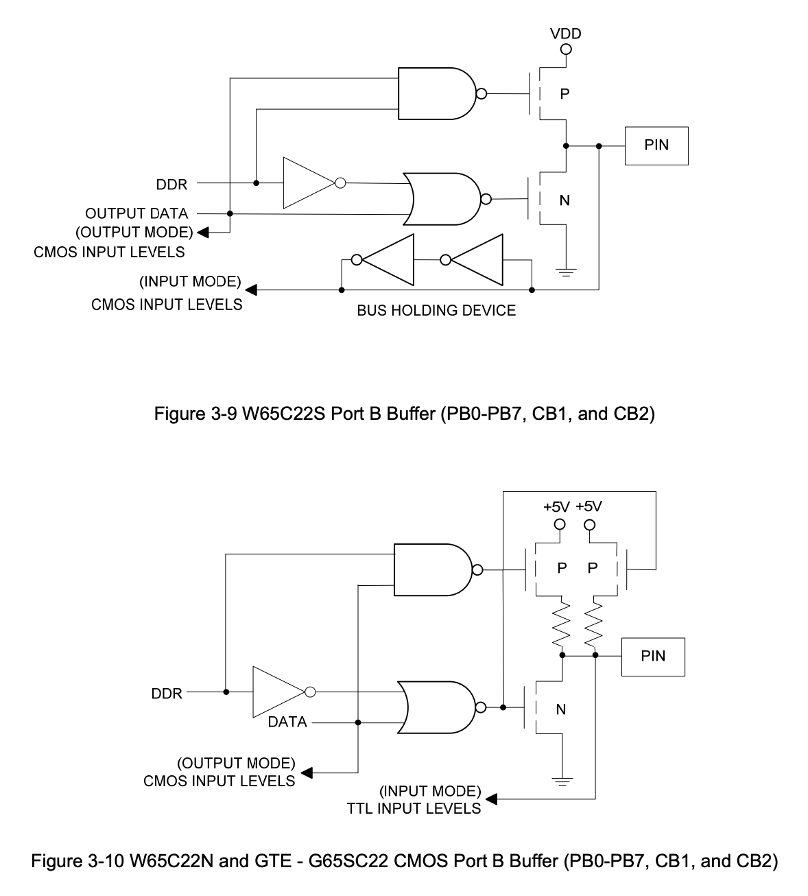
Apparently, IRQ handling is not the only difference between WDC65C22N and WDC65C22S. According to Adam (unfortunately, I don't have the former chip in my stock to confirm), the output pin was floating around 1.6V, since it was not being initialised as output. Or something like that, I might be mixing things up here. Here is the part from the datasheet describing the difference:
![]()
If you guys can explain to me why would pin float around 1.6V here in input mode I would be very grateful! I spent some time with this schematic and I think the culprit in WDC65C22N case is the right P MOSFET pulling the pin up when DDR is 0 (input), but would like to hear opinion of somebody smarter and more experienced.
The main point is still the same: something as small and seemingly insignificant as incorrect state of Blink LED was indicating much more serious issue of chip incompatibility. Luckily, thanks to Adam's remarkable perseverance, he managed to find the root cause and address it.
You have to remember - if you see something small that is off and don't think much of it, this might actually be something way more serious. As long as you are in prototyping mode, it's fine, you can come back to it later, but if you let that kind of detail slip into your final product design you might be in serious, serious trouble. Never ignore the "insignificant details"!
One more advice for the end
The main issue here is that on my PCB there was no place to solder in pull-up resistor for the VIA IRQ lines, it had to be done the hard way, by modifying the build a bit.
In future I will make sure that there is additional slot on the PCB where such pull-up can be installed - it just needs proper documentation in build notes.
And, while writing about it, there is another thing I learned recently. Some of the LCD screens, like the one I use (based on HD44780 controller) have current limiting resistor on their backlight LED, but that's not true for each and every single one of them. When using such LCD you will end up having much higher computer current usage and the display will be extremely bright.
I got really great advice for that from my friend: when designing port for LCD screen, just make sure to add footprint for additional resistor on the backlight power supply line. In case your user has the LCD screen with built-in resistor, they can solder in 0 Ohm resistor there (or simple jumper wire), and if they don't, they can install whatever they need for their specific screen. Great advice, isn't it?
-
The Gods of Electrickery have not been kind recently...
10/02/2020 at 14:11 • 1 commentCurrent status
Recently I promised to share the details of my rapid PCB prototyping exercise, and I wish I could do it being 100% certain about the results. Unfortunately, The Gods of Electrickery have not been kind to me recently, and I came across an issue that stopped me dead in my tracks.
As I wrote recently, the worst part of any project is when there seemingly insignificant things happen. Something works when it shouldn't, or doesn't where it should. Normal reaction would have been to shrug, rewire, reset and move on. Unfortunately, as I have learned the hard way, this is not a proper reaction. You should really get to the bottom of the issue for two reasons mostly:
- Chances are that it will occur again in less favourable environment (like, you know, production, or on PCB),
- Even if it doesn't, the Grand Issue is that you are supposed to understand your circuit. All the magicky stuff happening now and then is just your incompetence at play, and it will haunt you one day.
So, regardless of having at least three different solutions to the observed issue, I still don't know what happens and why these solutions work. To put it in proper context:
![]()
This is how I feel right now :)
Call for help
So far my blog here was all about triumph of a mind over matter; spectacular success after another. That makes writing this post all that harder - I'm stumped and I really don't know how to proceed.
Again, more than one reason to share. First and foremost, I really hope that some of you might have seen something similar and can suggest other ways to investigate (or to solve) the issue further. Help me understand what I'm missing here and how to approach cases like that. Teach me where I'm failing.
But the other reason to share is that I would like to send a message to all the beginners like myself who come across similar roadblocks. This is normal, you can't let it discourage you. You can choose how to approach the situation (apply the first possible solution, keep digging, or just move on regardless), but don't let that situation let you down.
And, even if you don't understand what's happening, there is plenty of investigation you can do on your own just using the opportunity to learn more about analysis and troubleshooting.
So, please, if you have any idea what might be causing issue that I've been struggling with or what else could I check, please let me know in the comments below.
The weird case of line wrapping
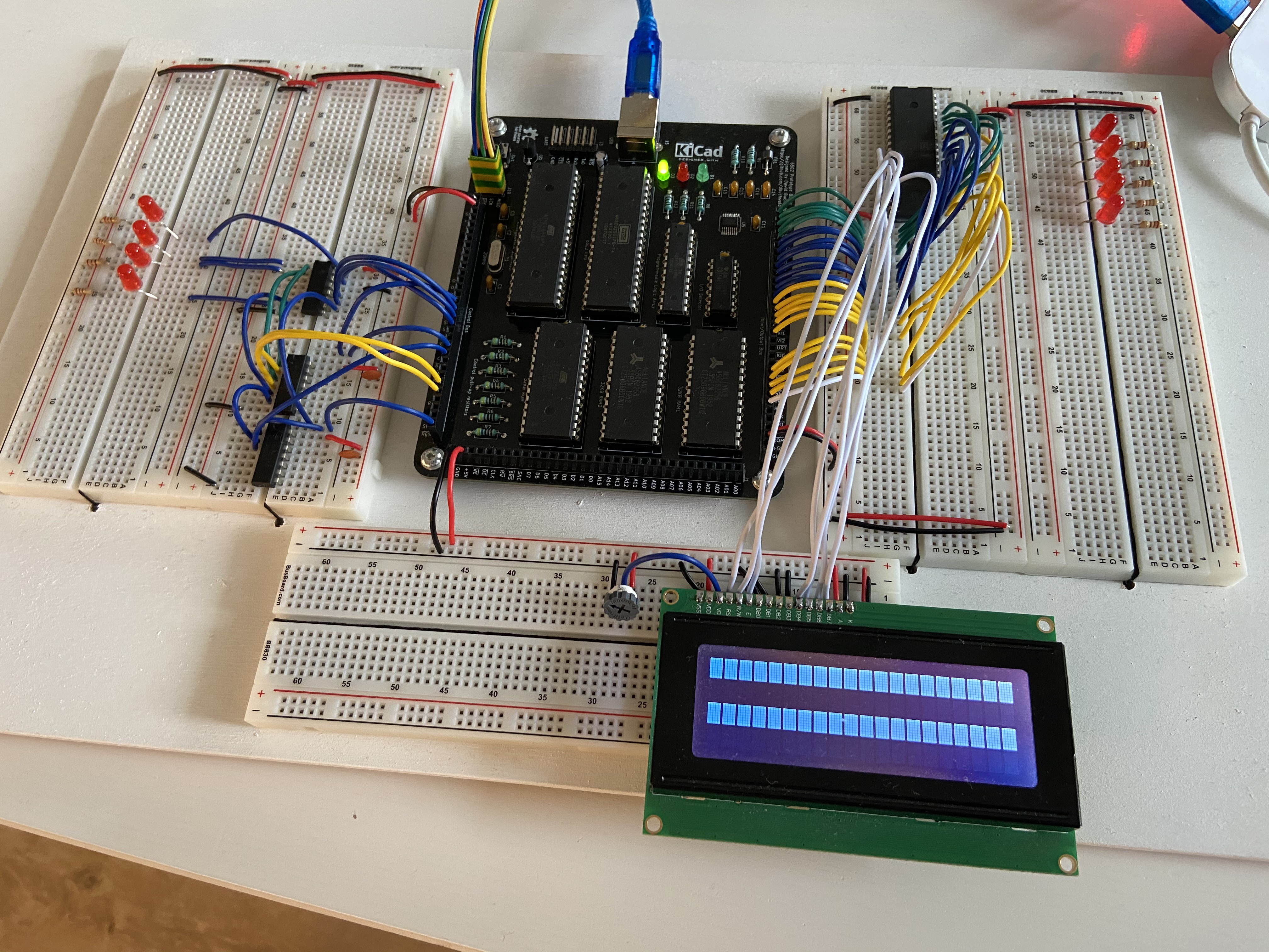
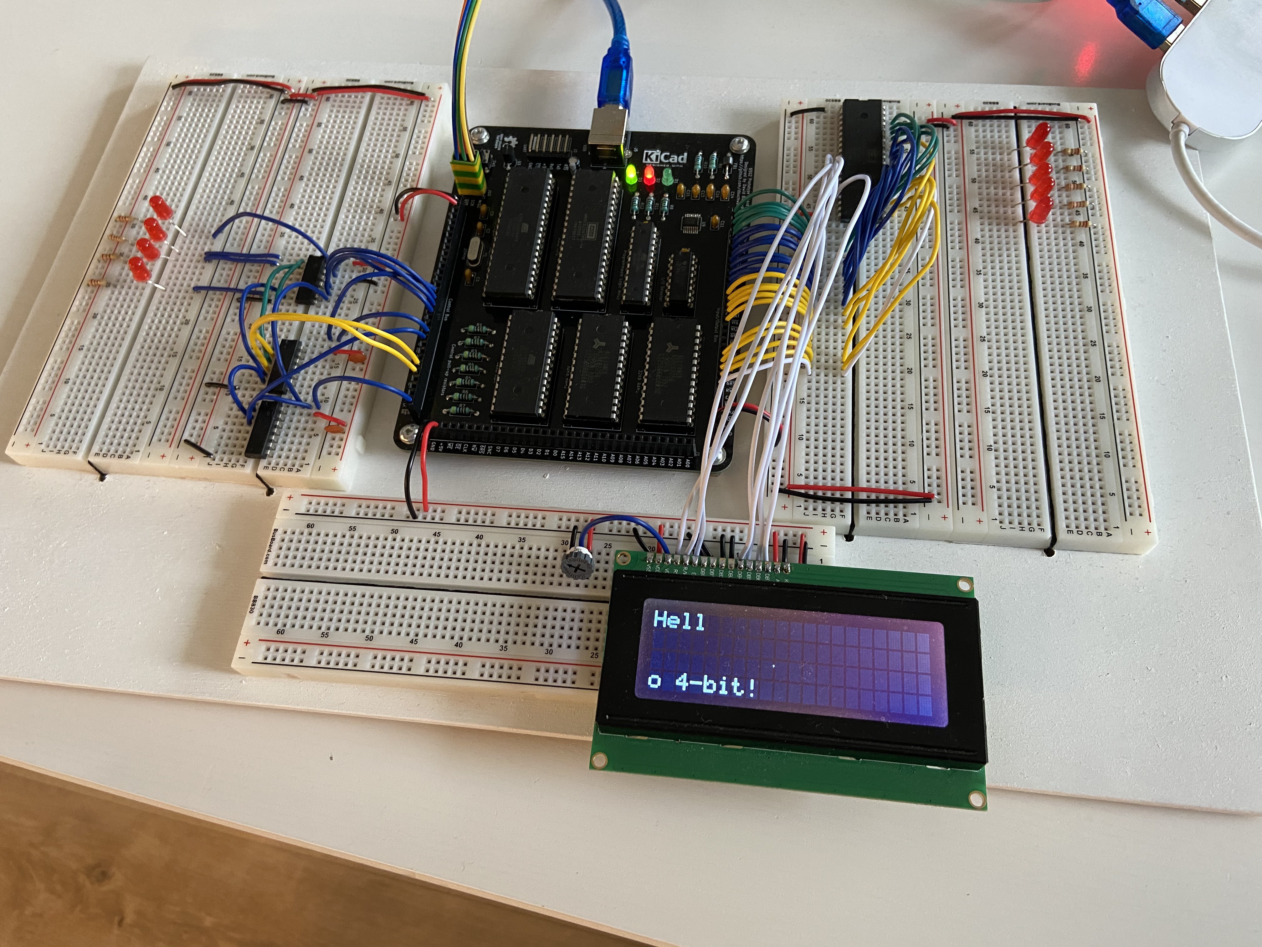
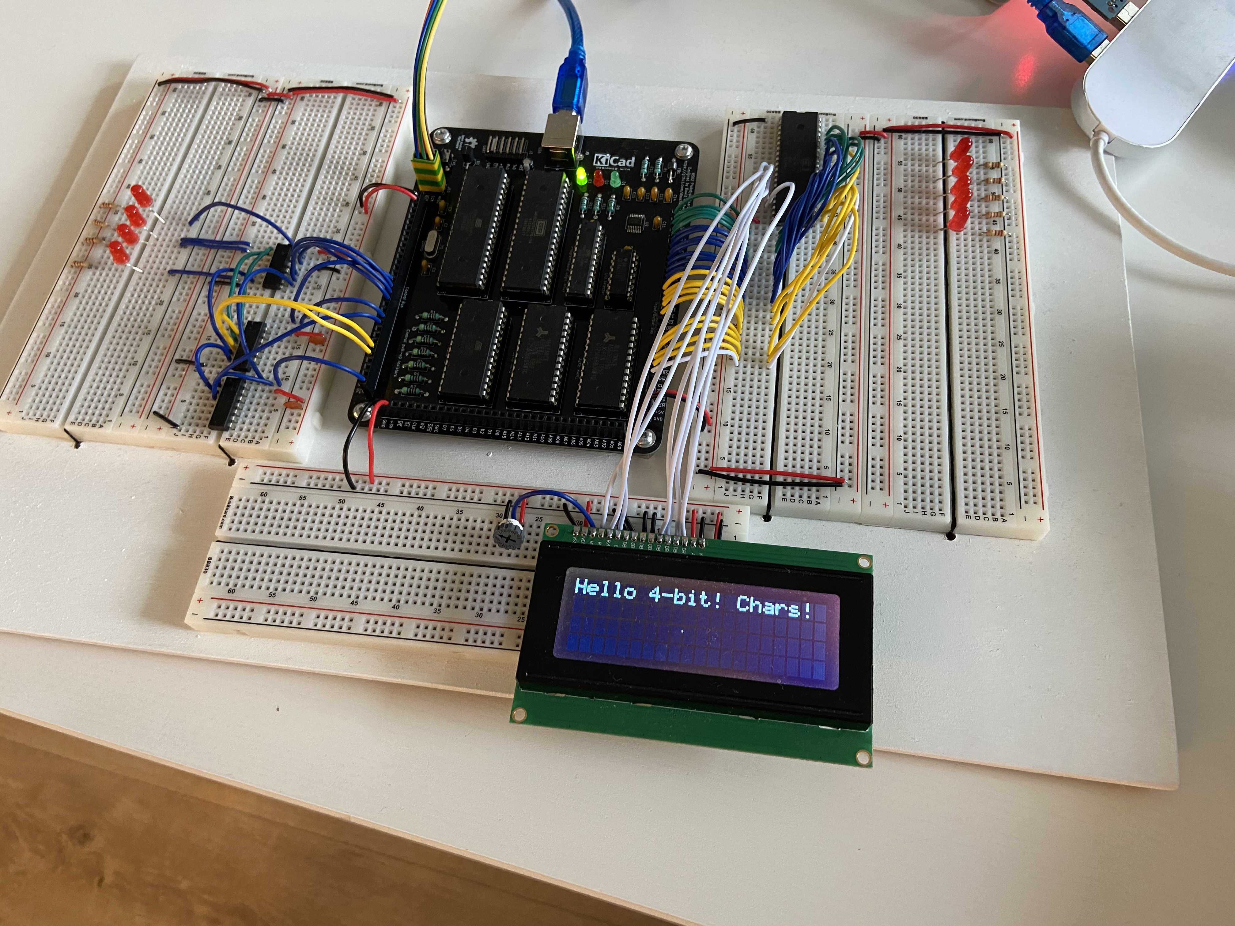
So, soon after receiving my DB6502 prototyping PCB (described here and here) and sorting out initial open questions (like feeding bus control signals from AVR to 6502) I started testing how the integration with external I/O components works. Plugged in my 20x4 LCD screen and ran some basic program to test it. The expected outcome was to display text "Hello 4-bit LCD! Chars!". I use 6522 VIA chip to interface to LCD. This is the basic setup:
![]()
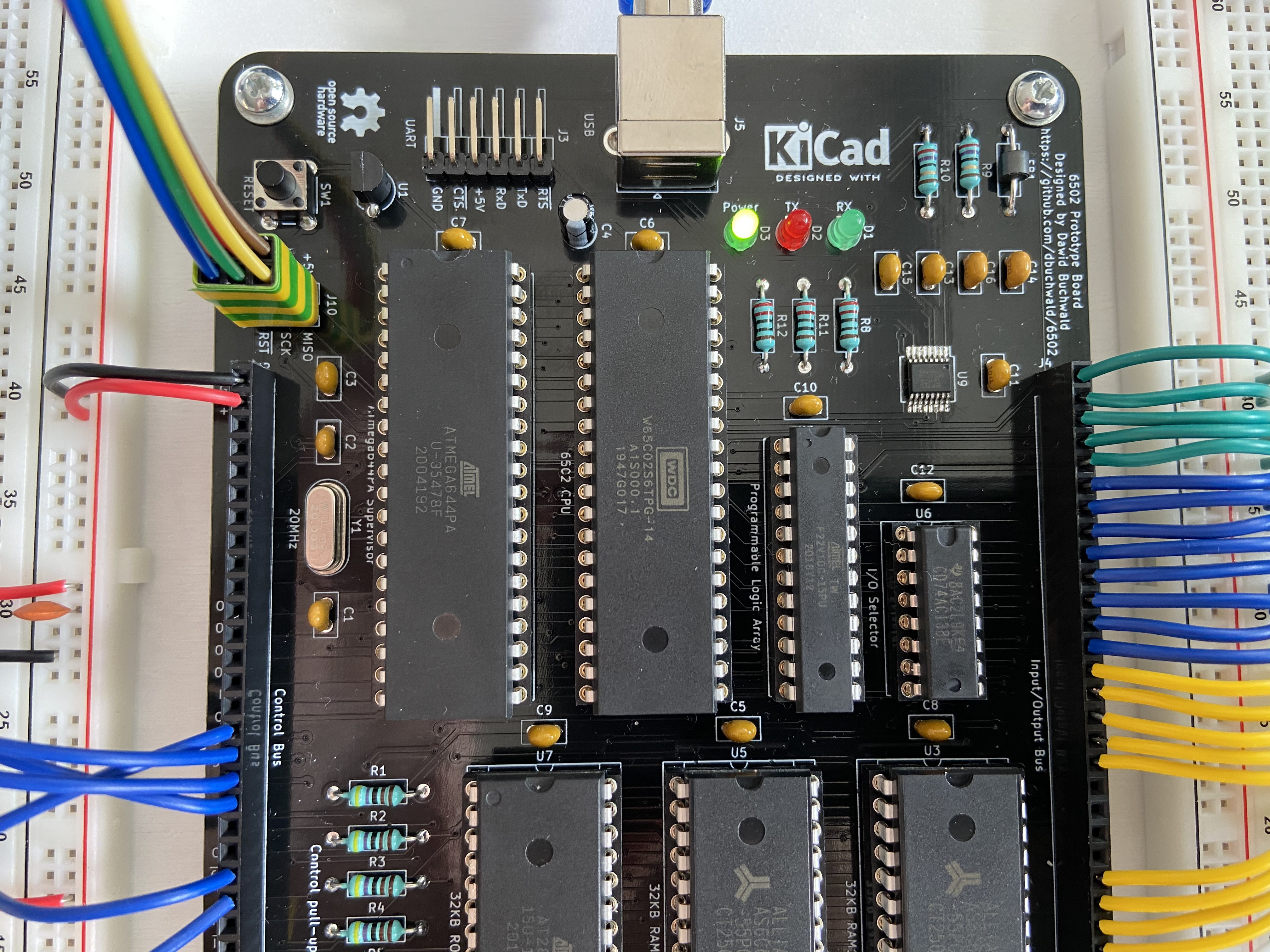
Now, to shortly describe what is here: in the middle there is a PCB with the core components: ATmega644PA used as a supervisor - it feeds clock input to 6502, can take control of system bus and flash the ROM chip. You can use it to step through 6502 execution (cycle by cycle) while observing system bus activity; 6502 CPU (the CMOS variant from WDC), two 32KB RAM chips (one not being used), 32KB ROM, ATF22V10 PLD for address decoding and 74AC138 for I/O channel selection.
Mandatory to run there are also several chips on the left side: 74HC595 shift register that AVR uses to control signals like RDY or BE for 6502, 74HC00 inverter for them and 74HC08 AND gate for RES signal routing (you can reset 6502 from AVR without resetting the latter). Pretty basic stuff.
On the right side there is a single chip - 6522 VIA (also CMOS variant from WDC) used to drive the LCD in 4-bit mode. As you can see, each of the breadboard sections is fed power and GND connections from three breakout ports on each side of the PCB.
Sorry, if all the above was a bit confusing, I didn't want to get into details, as I believe most of it is pretty irrelevant to the observed issue here. I will provide evidence explaining this reasoning below.
Get to the point, will you?
Right, to the point. Let's start with visual description of what really happens:
![]()
As you can see, text on the LCD has been wrapped incorrectly - after four characters there is a jump to last line.
Now, unless you have checked out my blog in the past, you might be thinking "this is just wrong LCD code", but that's not as simple as that. Please bear with me just a while longer, I promise it will get interesting.
I will describe the code that drives the LCD (and the details of the execution) in a more detail below when I discuss one of the possible solutions. I just want to present all the observations first to ensure proper context to this Electrickery Mystery.
Observation 1
One of the things very important to the issue at hand is that it occurs every single time. As long as the conditions are met (as in: without certain exceptions or "solutions" noted below) the problem will happen each time I run the code. There hasn't been any single case of corrupted characters, incorrect output, timing issues or anything of that kind. Execution is rock solid: display four characters, wrap to last line, keep going.
Again, you might be wondering why I don't just check the code. The reason is simple: the code is correct, I have the same code running in identical setup (but on PCB, not partially on breadboard) with speeds up to 8MHz just fine. So yeah, the code "should" work. Please, bear with me. And if you think I didn't check my code carefully, here and hereI wrote much more about it.
Observation 2
The picture above was taken when running 6502 CPU at relatively slow speed - few hundred Hz - while dumping all the bus activity to the serial. There is, however, alternate mode: you can run the CPU as fast as possible (up to around 800kHz), but then the bus activity is not written to serial output.
Guess what: running at fast speed prevents the issue from occurring.
![]()
There you go: the same hardware setup, different clock speed. No weird line wrapping occurs.
Please note: I have also tested the code in slow mode on another PCB-only build. The issue doesn't occur there either. This, most likely, is not timing issue. At least not as simple as it might seem.
Observation 3 (and Solution 1)
If you read my post about this particular PCB design, you know that it was sort of "quick and dirty" job. Not that it should matter at such a low speeds (even the MHz range), and the traces itself should not be that important. Having that in mind I tested what happens if I move the GND connection from bottom breadboard to one of the alternate boards.
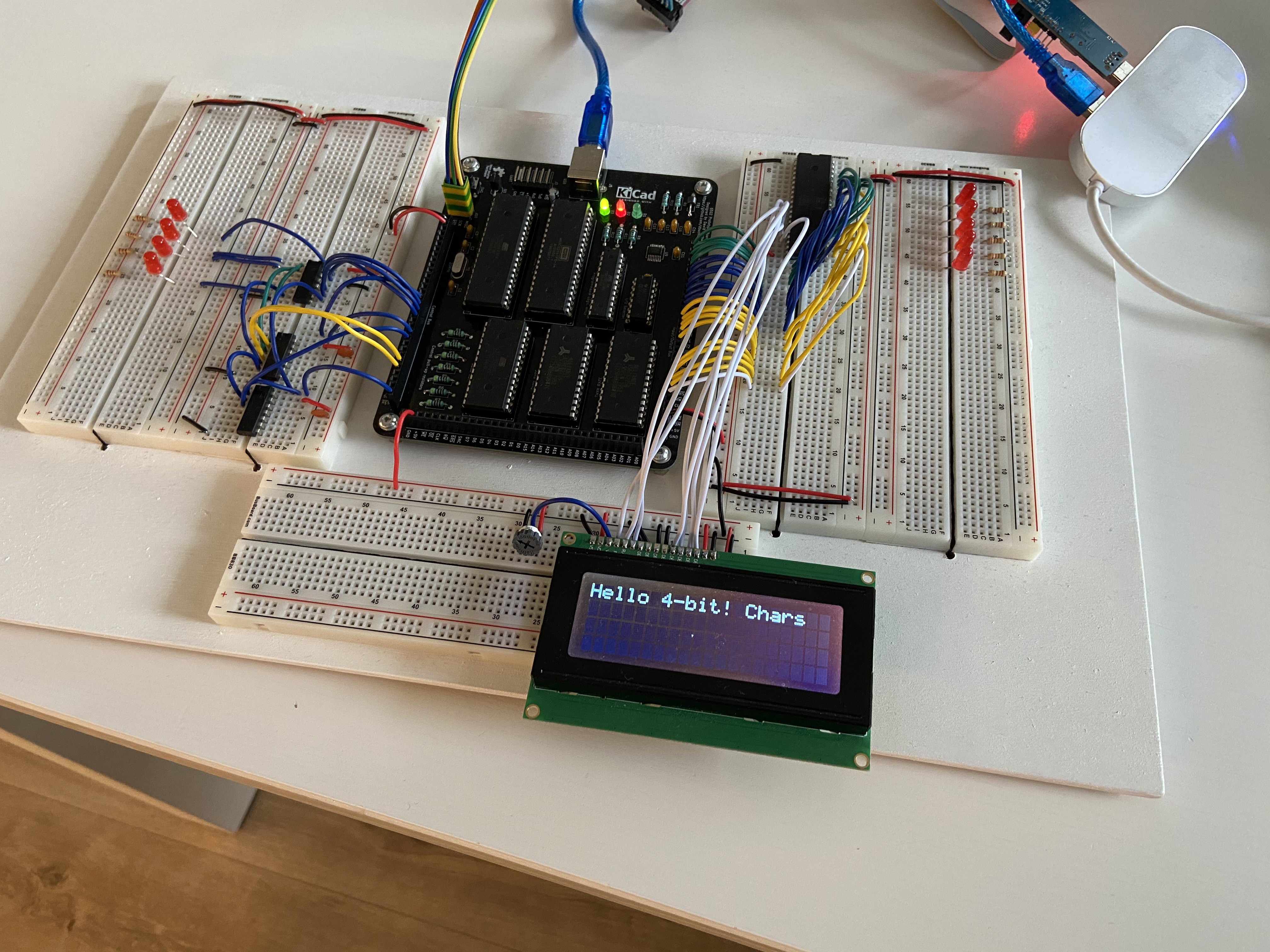
The reason I did that is that if you take a look at the build above, all the signals from the VIA come in the form of rather long wires (15cm+), while they are being referenced against GND level coming from the other side of PCB, near higher-frequency AVR clock (20MHz). So, I moved the black GND wire from between the PCB bottom connector and breadboard to connect the breadboards where the VIA signals are coming from (the right one):
![]()
You can see the black wire just above the center of LCD, hiding under the white signal lines. As you can see, the GND signal from the PCB bottom port is just disconnected.
And poof, issue gone. Tested about hundred times - each time it worked just fine. Slow, fast, no matter.
What I have also tested (but didn't take the picture of) was moving the GND connector to the left board, in theory making the route even longer - but it still worked just fine.
So, the observation is that whatever is causing the issue, it is somehow related to the GND connector on the bottom of PCB.
Now, I was tempted to stop there, but I wasn't satisfied with the explanation. Sure, if I put all this on PCB one day the traces will be shorter and the issue, most likely, won't occur again, but still: something is happening and I don't understand why. I mean if there is something wrong with the GND connector there I should be able to detect it or measure somehow, right? And there shouldn't be any other way to fix it, right?
Observation 4
So, it was time to measure what happens here. I grabbed my logic analyzer, plugged it right next to the Enable pin of the LCD and to the ground connector on the bottom BB. Moved GND connector to the old spot and ran the software again to catch the issue.
Nope. Not occurring. As if the presence of the logic analyzer itself was sufficient to prevent the issue from manifesting itself.
Disconnected the logic analyzer from the PC. Issue still doesn't occur. Disconnected GND connector of the LA, leaving just one single connection from LA to the Enable pin. Issue doesn't occur. Removed LA, leaving only the single wire connected to Enable pin - issue occurs again.
How do you solve something you can't even measure?!
Observation 5 (and Solution 2)
As you can see in the pictures above, I had handful of LEDs sitting there from the initial board testing. I grabbed one of the 220 Ohm current limiting resistors and I used it as pull-down resistor on LCD Enable line.
This solved the issue. I was so happy!
This explains it, I figured: after all, even logic analyzer probe behaves like a very weak resistor (1MOhm or so), so I was unintentionally pulling down the E line with it. Problem sorted, right? I rushed to the internets to confirm my theory and found interesting clue: all the lines on the LCD controller have weak pull-downs on them, with the exception of the E line. That was it then!
Or so I thought.
To make things nice and neat, I decided to use another, more appropriate pull-down resistor: 4K7. Guess what. The bloody issue returned!!!
Yes, you are reading this right: 220 Ohm pull-down prevents the issue from occurring. Logic analyzer probe prevents the issue from occurring. 4K7 resistor doesn't. Too weak?
And yes, in case you are wondering, I tested the 4K7 resistor - after all it might have been damaged and not conducting any current at all - and it was just fine, my meter measured 4.6 KOhm. F**k.
So, what I do know now? Something must be driving the E pin. If it was just stray capacitance or ringing on the board, 4K7 would have been strong enough to prevent the issue, right?
At the same time, the code should be fine if it's running correctly with just a minor tweaks to hardware (like moving GND connection or increasing speed).
I was just about to give up, but I figured there is another thing I haven't looked into: bus analysis.
Observation 6
So, I decided to look at the bus activity. I will not post full dumps here, they are way too big, so I will try to describe how the thing works from software perspective. If needed, I can provide the full logs on request.
The algorithm of driving these LCD controllers in 4-bit mode is pretty simple. Start with software reset operation, set up basic details and move on to data communication. This part is where it is interesting, and this is how the code works:
- Write single character to the LCD
- Start with reading the busy flag
- Read two nibbles of 4-bit each, starting with the MSB
- If the bit 7 is set, it means LCD is busy
- Repeat as needed
- Write single byte as two 4-bit nibbles, starting with the MSB
- Check for line wrapping condition
- Read current cursor location (after byte write)
- Start with checking busy flag before read operation
- Read two nibbles of 4-bit each
- Check bit 7
- Rinse and repeat
- Read current position from LCD by reading two nibbles of 4-bit each
- Compare read position against "wrap locations" - if match found, change address by writing another byte to LCD
- Start with checking busy flag before read operation
- Read current cursor location (after byte write)
- Start with reading the busy flag
This code has been tested in various configurations, at different speeds, with logic analyzer. It's basically bullet-proof. That being said, something must have been wrong with reading the position, because the line wrap happened too fast, and the resulting position wasn't in the next line.
After comparing system bus activity for scenario with or without pull-down resistor (or with different GND connectors) I noticed interesting discrepancy. The current position reads were not random in the faulty cases.
When GND rail was connected to another breadboard or the pull-down resistor of 220 Ohm was used, the consecutive reads of current cursor position after writing each character were, as expected:
01, 02, 03, 04, 05...
Now, the same operation without the pull-down and with GND connected to the bottom of the breadboard would read:
10, 20, 30, 40, 55, 65...
See the pattern? It's like there is an 4-bit offset in the operation. As if there was single, unintentional read at the beginning of the sequence, so instead of 01, 02 it reads 10, 2... Finally it reaches 40, and this is the signal to move to the last line - location 54 - which is correctly executed, followed by read 55 and 65 (55 and 56 in reality).
I figured I had to look for one single rogue signal that would raise E line shortly after reset sequence completed - that would explain the 4-bit offset.
Then I came up with another hypothesis to test: see what happens if I disconnect the pull-down resistor after first characters are written?
Observation 7 (and Solution 3)
So I had it mostly figured out: something happens after LCD init operation causing single random spike on E line, and it's interpreted as 4-bit nibble read operation. If I prevent it with my pull-down resistor for long enough, it should be fine, right?
So I did. Ran the code slowly, with the pull-down connected, until the first 'l' character ('Hel' displayed on the screen). Then I paused the execution, disconnected the resistor and resumed execution.
Problem occured again.
Checked system bus log, and the reads were invalid again:
01, 02, 03, 40, 55, 65...
So, as it turns out, the weird "read" happens every cycle. With every single character.
What's more interesting, is that theoretically the 4-bit offset should manifest itself in the busy flag checks as well - after all this is reading from the same register. It doesn't. While checking busy flag I can't see the offset - it's always read correctly, with leading zero (or five after wrap).
Started investigating the code even further, and came across something that could be described as inefficiency. Before each operation (write/read) I change the direction of the subset VIA port by writing to DDR register. For usual operation this is how it looks (compare algorighm above):
- Toggle to read mode (write 0x0e to DDR)
- Read busy flag
- Toggle to write mode (write 0xfe to DDR)
- Write character data
- Toggle to read mode (write 0x0e to DDR)
- Read busy flag - this works fine
- Toggle to read mode (write 0x0e to DDR)
- Read current cursor position - and this does not
As you probably noticed, there is one unnecessary write to the DDR: toggling to read mode in the last step, just before reading the current cursor position. That being said, it should not change anything, because 0x0e is the actual content of the DDR register:
/read
  0222: r 0e
  0222: W 0e

/bf-no
  0220: r f4
  0220: W 04
  0220: W 0c
  0220: r 0c
  0220: W 04
  0220: W 0c
  0220: W 04
  0220: r f4

/write
  0222: r 0e
  0222: W fe

/Letter 'e'
  0220: W 62
  0220: W 6a
  0220: W 62
  0220: W 52
  0220: W 5a
  0220: W 52

/read
  0222: r fe
  0222: W 0e

/bf-no
  0220: r f2
  0220: W 04
  0220: W 0c
  0220: r 0c
  0220: W 04
  0220: W 0c
  0220: W 04

/read
  0222: r 0e
  0222: W 0e

/position 20
  0220: r f4
  0220: W 04
  0220: W 0c
  0220: r 2c
  0220: r 2c
  0220: W 24
  0220: W 04
  0220: W 0c
  0220: r 0c
  0220: W 04
This is (filtered to VIA access only) system bus log of one of the executions. You can probably see the last DDR write:
/read
  0222: r 0e
  0222: W 0e
Does it make sense? No, not really, but the alternative would be to read it, manipulate bits as needed (there are certain calculations required, since one line in this port is not related to LCD), then read again to compare if change is needed, and write only if it really is.
This is the original code:
        ; Preserve direction of last four bits of DDRB
        ; but toggle LCD data lines to input
        lda LCD_DDR
        and #(BLINK_PORT_MASK)
        ora #(LCD_DDR_READ_MASK)
        sta LCD_DDR
And this is the same code with the modification:
        ; Preserve direction of last four bits of DDRB
        ; but toggle LCD data lines to input
        lda LCD_DDR
        and #(BLINK_PORT_MASK)
        ora #(LCD_DDR_READ_MASK)
        cmp LCD_DDR
        beq @no_change
        sta LCD_DDR
@no_change:
I guess you know where I'm going with this, right? This solved the issue again. No pull-down required, no need to move GND connection elsewhere.
What's the problem then?
Well, the problem is that I'm not satisfied. There is no reason the VIA chip should behave this way, and even if it was, it would happen regardless of clock speed or GND connection layout. If the pull-down was required, then 4K7 would be just as good as 220.
And, what's worse, I should be able to observe the issue somehow. It would not disappear with single probe of LA attached.
You might be wondering why I haven't used scope to investigate. For one, I don't have it. At least not a proper one, all I have is a simple Hantek 6022BL USB toy that I borrowed couple of months ago and haven't even opened the box yet.
This seemed like the right moment to use it, and I did. I tried connecting it to E line next to the LCD, but this stopped the issue from occurring. When I moved the probe to the VIA side, the issue would keep occurring, but there was literally nothing on the scope that would look out of norm. Just a regular, clean signal.
Maybe the scope is crap (I mean I do know it is :)), but I can't really justify such an expense without being certain that the proper DSO would help me troubleshooting this. I mean it's nice to have scope and all, and my birthday is coming soon, so the excuse is there, but if I can't use it to solve problems then maybe, just maybe, I don't need one.
HELP PLEASE :)
Please, if you have any idea what I should try next, what kind of test should I run to test any other hypothesis, then please let me know in the comments below.
I know I have solution of sorts (actually, three of them so far), but it's not the LCD that I'm troubled by. My problem, for which I humbly request your assistance is in understanding what else can I do to get solid understanding of the underlying phenomena here. All help, clues, questions will be highly appreciated!
Thanks a lot in advance, and may Gods of Electrickery be kind to you :)
-
Tech quickie - USBAsp and fresh AVR chips
09/28/2020 at 16:12 • 0 commentsJust a quickie
There are some steps in my project that take a lot of time and effort to document, and I love writing about them. There are, however, small issues, problems, obstacles that don't require full-blown post to describe, and yet I want to share them because they weren't that easy to research online. I will call these tech quickies and document them in much shorter posts.
Using ICSP for AVR chips
Since my first version of 6502 computer, I loved the idea of being able to program AVR controllers directly on the board without the necessity to remove them. I was really proud of myself when, almost at the last minute, I added the port for it on my board, and it worked perfectly.
For me, that is, because some people complained about it, and they were right. Depending on the programmer you use and the origin of the chip it might be trivial or not so much, so lesson learned here. Consider how it works with fresh chip, be mindful of default fuse settings and quirks of different programmers.
Some time ago I built simple POV toy for my son (I mentioned it recently) and it is basically ATmega168P + some LEDs that blink very fast to make nice images when waving the thing in dark room.
![]()
Now, when I built it on protoboard, I plugged in one of fresh ATmega168 chips (purchased just for this project specifically), plugged in my USBAsp programmer and tried programming it:
➜  ~ avrdude -p m328p -c usbasp -P usb  -t

avrdude: error: program enable: target doesn't answer. 1
avrdude: initialization failed, rc=-1
         Double check connections and try again, or use -F to override
         this check.


avrdude done.  Thank you.
Please note: this is not the exact command I used (this comes from further investigation), the original session output got lost in the fight.
I have seen this one before
This reminded me that I have seen these errors before, and the way I solved them, after some head scratching, was basically to use Arduino Nano as ISP programmer. I remember doing some research online and just came to conclusion that I still don't know what it is, but using Arduino ISP and external crystal solved the problem.
Since I wanted to complete the toy project this was exactly what I did again: fished out the chip, put it into the breadboard, programmed there with Arduino ISP that didn't seem to have any problems with the chip.
It kept bothering me though. I hate to not be able to understand why something works or why it doesn't. I hate workarounds that don't address the underlying issue, they just obscure it so much that you forget what the actual problem was. And if you have ever ran into these issues with USBAsp, I bet you found these approaches:
- Replace your AVR, because it's bricked,
- Connect external crystal + 22pF caps,
- Add capacitor to reset pin,
- Remove capacitor from reset pin,
- Throw a handful of caps at various pins in different locations,
- Get yourself another programmer,
- Update USBAsp firmware and/or Windows driver (if using),
- Connect external power to your board, as USBAsp is not providing enough voltage/current.
Now, these are nice advices, but none of them has anything to do with the problem. And, more often than not, these will not help at all.
How to troubleshoot it then?
Well, what I noticed is that once I got the first programming out of the way with Arduino ISP, the problem never occurred again, making it more difficult to investigate. As if there was some kind of magical formatting needed that the USBAsp wasn't capable of. I didn't like the explanation, especially because I wanted to start using SMD version of ATmega chips, and these you can't "fish out" of your board for breadboard programming. Somehow it never occurred to me that maybe I could use Arduino ISP with the onboard ICSP port. Well, brain is a funny thing :)
When purchasing some other chips for my project recently, I decided to put an end to the whole debate in my head. Get handful of fresh AVR chips, replicate the problem and instead of rushing to workaround, keep banging my head against it until I figure out the actual underlying problem and find proper, kosher solution to it. I'm happy to share that I managed to find and solve the issue once and for all.
So, what is the real problem here?
Now, to find the solution, you have to understand the problem here. Sadly, it's stated clearly on the USBAsp project website, but somehow Google got overran with the above advices, making it all too hard to find a link to observed problem.
SCK option to support targets with low clock speed (< 1,5MHz).
Now, why is that important?
The problem is that AVR chips have inbuilt oscillator running at 8MHz, but by default this frequency is lowered to 1MHz using inbuilt clock x8 prescaler. This is just how these are set up in the factory.
Sometimes when you buy them, they have already Arduino bootloader installed and their fuse configuration is changed to not use the prescaler anymore, and they run at full 8MHz. Sometimes you get used chips that have already been configured to use external crystal and simply won't run without one on breadboard, but if you add it, they will run at full speed of the crystal, probably 16 or 20 MHz not causing the issue anymore.
But, what is important here, default configuration of factory-fresh ATmega328 or ATmega168 or ATmega644 (these are the ones I tested it against) is to run at 1MHz using internal 8MHz clock and x8 prescaler.
This is just too slow for USBAsp. ISCP protocol uses SPI interface to transmit data, and USBAsp uses too high clock rate (384KHz I believe) for chips running at 1.5MHz or less. Arduino ISP apparently uses lower SPI speed or addresses the issue in some other way.
Point is: if your USBAsp programmer complains about target not responding start with checking if slowing it down helps.
Proper solution
What doesn't help is that it's also not so very clear how to reduce the programmer speed. If you are using AVRDUDE, the option is -B n where n is by how much the SPI clock should be slowed down. This is where I found the solution, and it suggests to use factor of five. You can experiment with other values.
Unfortunately, this is what the help says:
➜  ~ avrdude
Usage: avrdude [options]
Options:
  -p <partno>                Required. Specify AVR device.
  -b <baudrate>              Override RS-232 baud rate.
  -B <bitclock>              Specify JTAG/STK500v2 bit clock period (us).
  -C <config-file>           Specify location of configuration file.
  -c <programmer>            Specify programmer type.
  -D                         Disable auto erase for flash memory
  -i <delay>                 ISP Clock Delay [in microseconds]
  -P <port>                  Specify connection port.
  -F                         Override invalid signature check.
  -e                         Perform a chip erase.
Now, I still don't know why I have to use option that is described as JTAG/STK500v2, since I'm not using any of those. And, to be fair, it has nothing to do with microseconds either.
This is what happens if you provide the proper option:
➜  ~ avrdude -p m328p -c usbasp -P usb -B 5  -t

avrdude: set SCK frequency to 187500 Hz
avrdude: AVR device initialized and ready to accept instructions

Reading | ################################################## | 100% 0.00s

avrdude: Device signature = 0x1e950f (probably m328p)
avrdude> dump lfuse
>>> dump lfuse
0000  62                                                |b               |

avrdude> dump hfuse
>>> dump hfuse
0000  d9                                                |.               |

avrdude> dump efuse
>>> dump efuse
0000  ff                                                |.               |

avrdude> dump lock
>>> dump lock
0000  3f                                                |?               |

avrdude> quit
>>> quit
Much better, isn't it?
When using Arduino IDE, you can select specific variant of programmer (slow one):
![]()
Side note - burning the bootloader
One of the issues I had (or rather - people who built DB6502 version 1 had) was that if they installed fresh ATtiny4313 in the board for PS/2 connectivity it would work extremely slow (or not work at all). As it turns out, these chips have exactly the same issue: in order to make them work with the provided Arduino sketch you have to "Burn Bootloader" to them. And, what's funny, it has nothing to do with the bootloader itself - this is where the "set up AVR fuses" option is hidden in Arduino IDE.
So, the key message here is: keep in mind the default setup of fuses in your AVR chip, and if for one reason or another you expect the user of your project to use non-default settings, provide them with instruction how to change it. If you expect them to use USBAsp, and the default setting of your chip is to run below 1.5MHz, note this hint as well!
-
Rapid PCB prototyping - update (part 1)
09/24/2020 at 18:37 • 6 commentsWhat is your excuse?
This header title of this section was supposed to be separate post on its own. One of the first things that surprised me when I started working on DB6502 version 1 design was the general hesitation for SMT soldering among beginner EE community. I did feel a bit intimidated by it as well, but I couldn't find UART->USB converter chip in DIP package, so I settled for not-so-beginner-friendly FT230XS in TSSOP-16 package. Got myself couple of chips, several adapters and while waiting for the delivery started watching YouTube videos about the process.
OK, it didn't seem trivial, but didn't seem that hard either. Then I came across this excellent post (which I, obviously, lost) where somebody proposed slightly different procedure. Since it seemed the most reasonable to me, I decided to give it a try.
Then the chips arrived. Much smaller than I expected :) Not to worry, I got to work. My first attempt at TSSOP-16 was horrible, I almost burned the chip, adapter and my apartment.
That being said, it actually turned out OK. After about an hour of experimenting with flux, wick, solder and different soldering tips it looked fine and worked as expected.
That's not hard, I thought to myself, and started with a second chip. Took me only five minutes. Later got myself SMT practice board (they are cheap and contain various footprints) and spent some time with it as well.
Recently, when playing around with the idea for DB6502 I wanted to try out some specific chips that, sadly, are not available in DIP package. I figured it would make nice post for my blog, where I would show the process. To get better light I moved to terrace on a sunny, exceptionally warm day. Long story short - I was sweating like a pig, cursing like a seaman, but hell-bent on making it happen. Took plenty of photos, soldered several chips. Moved inside to check out the pictures just to find out that most of them were utter shit. It was so bright I didn't notice they were out of focus... Here are some before and after:
![]()
![]()
Oh, and out of the above, only one pin was not connected correctly. There were no bridges. All in under an hour.
What's with the excuses then?
Well, actually two things: for one, my crappy pictures aside, there is no excuse really to give up on SMT soldering. You should try it, and I will demonstrate the process I use below. Now, I understand that some people can't do it due to physical conditions, sometimes caused by age or other diseases, so if you suffer from them, don't take it personally. I'm addressing here the healthy majority, especially younger engineers - guys, man up, try this. It might turn out easier than you think.
But I do have second takeaway from the story: as usual, I want to emphasise the importance of sharing with others. Working on a project? Share your stories. People will notice and they will give back. Recently I was contacted by another Hackaday user and he informed me that there are actually UART->USB adapter chips in DIP package. It's MCP2221A, and I will write more about it soon. Bottom line: what's your excuse to not share your work?
Back to business, what about these PCB prototypes?
Again, this post is not sponsored by PCBWay, but I just have to recommend their service. The whole process (order validation, manufacturing, shipping and delivery) took under a week. This is really fast, and it ties perfectly in the "rapid prototyping" flow.
What about quality? Glad you asked:
![]()
Lovely :)
First things first: FT230XS soldering
So, what's the secret procedure I use?
First, soldering station: doesn't have to be something fancy. I use Zaoxhin 936DH with 1C Black tip. 340 degrees Celsius. Flux pen. Thinnest solder you can find - I use 0,56mm. That's it, really.
Now about the process up close:
![]()
![]()
![]()
This is clean PCB, nothing happened yet. Sorry for pictures quality, but these are really small, and pictures have been taken with my phone...
Now, apply some flux. "Flux is your friend" - remember that, it will be your mantra for forseeable future. It will help you, and it's important you understand what it does, because it has two important properties. For one, it makes solder flow easier (original entry claimed that it lowers the melting point of solder, which is not true, sorry for this!). This makes it easier for solder to flow where it's needed. And the second property is even better - it cleans the surface of copper, making the solder easier to attach. As a result, flux will ensure that your solder flows and it flows exactly where you want it (on the pads and pins) and not elsewhere (on the soldermask or between the pins). Pure magic!
So, what's the appropriate amount of flux? Beats me, but this is what I give:
![]()
Now, the conventional wisdom says: put some solder on one-two pads, attach the chip to them, take more solder and put in on remaining pins, and if there is too much, use wick to get it off. Now, maybe it works for you, but I prefer to do it differently. Mostly because wick and thin traces/pads (typical for TSSOP package) don't mix well. If you let the wick attach to the pads and try to pull it off, you might rip off the trace. Don't do it, and remember, you have a friend that makes solder flow better. Guess what helps when removing solder with wick :)
Put some solder (just a little tiny bit) at the end of your cut tip like so:
![]()
![]()
![]()
Then smear this small amount of solder on all the pads, so that very, very thin film of solder covers them:
![]()
![]()
![]()
I bet you can't see the difference in these pictures, but you will see it if you do it. The pads are just a little thicker, that's it. You don't want them too thick, because the next step will be much harder.
Actually I did find two photos that should illustrate the difference before and after (these are from the terrace incident I mentioned previously):
![]()
![]()
Place the chip on the pads. Take all the time you need to place it as nicely as possible:
![]()
![]()
Are you ready for grand finale? The most difficult part will be soon over, and this is really trivial. Take your soldering iron, and if there is any solder or other crap on it - clean it on the sponge. Using your pliers (finger if you are brave or whatever), press the chip in place so it doesn't move when touched. Using clean soldering tip (and no solder!) just touch each of the pins for a second or two. Solder on the pads will melt and secure the chip in place.
![]()
That's it, you are done. Congratulations. Wasn't that hard, was it? I had my wife (no experience in EE whatsoever) observe the process and she was genuinely surprised how easy it turned out to be.
Oh, and if you see bridges in the last photo, you are right, but they were there from the beginning, it's part of the design :)
Now, I don't know, maybe this process has some flaws. Maybe it's not kosher enough or whatever. The thing it works, and it prevents many issues like bridges or thermal damage.
One more note about QFP package (or any other package with more than two sides to it) - it's a bit harder, because you have to align the chip in two dimensions, so the procedure is slightly different. Start the same, put flux on all pads, take some solder to the tip of the iron, apply it to the pads. Then position your chip the best you can and when you think it's as good as it gets, secure it in place by touching just one pad on one of the corners. Put the solder iron away (clean it!) and check the alignment. There are two options: it's OK or it isn't. If it isn't (and probably won't be the first time), see if you can correct it by nudging the chip a little. If it works, move on, otherwise just touch the same pin with solder iron tip again and pull the chip gently - it will detach and you can try again. When you finally get the alignment OK, just secure it in place by heating up one of the pins on the opposite corner and then just move pin by pin, heating them up and locking in place. Easy-peasy:
![]()
Now, you might be thinking I post about it just to brag, and sure, to some extent I am :) Still, the key message is the same: it's not as hard as it seems and it's very useful skill. You can use smaller, single gate chips. You can design significantly smaller boards. You can put your chips on both sides of them. It would be a shame not to try.
What have I learned from the PCB prototyping lesson
Well, it will probably take me a week or so before I can test all the possible connections on the board and be able to say with 100% certainty whether it's correct or not. That being said, I have ran some tests on it already and it turned out OK. I will post the results below, but I would like to start with the most important errors I made and what I learned from them.
Just check the bloody schematic!
Seriously, I wrote about it last time. It takes just one second, one critical review, to notice the schematic was wrong. D+ connected to D- and vice versa. Seriously. I should have looked at it, and I would have noticed it immediately. Thing is I was trying to be super-fast, just to see how many mistakes I make.
Turns out I'm not perfect. Need to double check!
Cutting the traces is actually hard
Obviously, there was simpler way to fix the above problem. I could have soldered the resistors between USB port and FT230XS cross-wise and that would be easy. It wouldn't look nice, but would get the job done.
Then I thought to myself - come on, try the cut and patch method, you have never tried it. See what happens. Famous last words :)
![]()
So I tested the continuity (to remember which trace goes where) and I cut the traces with wallpaper knife. Tested again for continuity. Beep. WTF?
Checked schematic to confirm that I'm cutting the right trace. I am. Cut again then:
![]()
Beep. Beep. Beep. Cut. Cut. Cut.
![]()
Silence. Silence. Silence.
What follows looks like a crime scene. I was right to decide to do it underneath the USB port so my shame is hidden forever (and yes, I did check the port to confirm there is no conductor there to short the cuts):
![]()
The important lesson here is that traces are not as fragile as they might seem. It takes deliberate action and quite a lot of effort to damage them. The main exception, obviously, being the solder wick accident, but it's also avoidable as long as you are gentle when pulling the thing.
Make notes!
Remember how I checked which trace goes where before cutting them? I made it specifically to ensure that when I solder the patch wires below the board, they connect the right pads. I didn't note it down, because how could I forget, I'm not that stupid, right?
I think you know where this is going. Seriously, I'm not making this up, I really did solder them exactly the same way as the original traces were. I guess I am that dumb after all :)
MAKE. THE. BLOODY. NOTES. MAKE. THEM. NO. EXCUSES.
Patches on PCB don't look THAT bad
Sure, it looks better if there are none, but is it worthy months of perfecting? Nope:
![]()
And the point is: I learned a lot. I guess you have to make mistakes to learn, right?
Follow your gut feeling
There was one thing I noticed when I generated the 3D view of the board in KiCAD. I wonder if you noticed that too:
![]()
There is something off here. The ISP connector should be male, not female. I did notice it, and I was like "whatever, it's just 3D footprint, it doesn't matter". Well, as a matter of fact it does. This is what I placed on my board:
![]()
And this is what I should have placed:
![]()
See the difference? Female socket is the mirror reflection of the male one, and for a good reason - so that when you plug the latter into the former, the pins line up perfectly.
And, to make things worse, all I had to do was to pick up the board I had laying around and see that again:
![]()
All I needed to do was to lean forward, open the drawer, pick that up and compare. I should have done it.
Was it hard to fix? Yes and no. Yes, because I just built an adapter to my USBAsp programmer that reverses the sides of the connector. Just a couple of male-female hookup wires and some tape to keep them together.
The problem, however, was that it might have not been that easy. If it was intended for a shield connector, I wouldn't get away with it that easily, and fixing that with cut and patch method would be much, much harder. No way to hide the cuts either.
And from the perspective the worst part is that I did notice the weird footprint. I had my gut telling me that maybe there is something wrong, but I ignored it. Key takeaway: never ignore your gut!
Vias and silkscreen don't mix well
On a PCB design it looks innocent:
![]()
But in reality, it doesn't look that nice anymore:
![]()
Is it cosmetic? Yes, sure, but it might make a lot of difference, making your silkscreen confusing or illegible.
Consider the usability of the board
When I placed these "edge" connectors on my board, I wanted to make sure each of the 96 pins is described correctly:
![]()
What I didn't consider was that the wires plugged into it would be going outwards, over the labels, effectively obscuring them:
![]()
Again, this is cosmetic issue, but the board would be better, more usable, if I just moved the labels to the other side of the connectors.
Think again about that usability
I placed IRQ and NMI connectors together with the BE and RDY signals on the control bus. For some reason it never occurred to me that I might actually need them also on the other side of the board - in the I/O port section. After all, this is where most of the interrupts come from :)
Yeah, it's a minor one, and all it requires is just one really long wire, but still. Stupid and avoidable with a little bit of consideration.
So, was it worth it?
Hell yeah! I made some really silly mistakes, learned the limits of the process. Now I know that next time I will check these details carefully, but I will not spend months perfecting my design. Ugly traces are invisible under soldermask, and even if they were visible, it doesn't matter.
![]()
What does matter is that within a week I managed to test some of my ideas that would take long long weeks on breadboard and probably even longer on perfboard.
![]()
And man, this development process now is wonderful: plug the thing into USB port, upload ROM image in just a couple of seconds, step through the code and reset as needed.
![]()
Supervisor firmware is still in very early stage, and there is quite a lot of work ahead of me to test all the features I had in mind, but it's really pleasant experience now, and finally I can move forward with DB6502 version 2. I don't have to worry about most of the wires, interfaces to external chips (like UART of VIA) are simple and limited to minimum. The whole thing is secured with prototyping breadboards to piece of plywood so I can move it around my apartment as needed without the worry of cables falling out.
Finally I can experiment with wait states, DMA, ROM/RAM banking, multi-CPU architecture (already on the board, mind you!). All of that within one week. Totally worth it!
Oh, and in case you are interested - I will be sharing the protoboard design and BOM on PCBWay and GitHub so you can get your own if you want, but before I do that I need to make sure that all the connections work and I have answers to some of the open questions.
In the meantime stay tuned, I will be sharing more updates soon. Let me know what you think in the comments below!
-
Rapid PCB prototyping and what can possibly go wrong?
09/18/2020 at 18:32 • 0 commentsBreadboards - the worst of best inventions ever...
When I first started contemplating getting into field of hobbyist electronics, it was the discovery of breadboards that sparked my interest. I understood that they are the magical devices that are perfect for all hackers and tinkerers alike. Devices from alien galaxy that allow you to build complex circuits that are pretty robust and yet completely modifiable over time. I loved the idea, but then I came across some book about beginner Arduino projects and couldn't understand pull-up resistor concept. It just didn't make a lot of sense, so I got into ceramics instead and spent couple of years on it.
Then one day I stumbled across first Ben's video about 6502 and I decided to give electronics another try. Maybe it was because he made me understand what the bloody pull-up is, or maybe it was simple childhood nostalgia about my Atari 800XE with tape drive.
One way or another, I started playing with breadboards. I really considered them the best invention ever! And they probably are, until, that is, you purchase Ben Eater's 6502 kit and try to wire CPU, ROM and RAM and Arduino Mega debugger on a single breadboard with AWG22 wire. And then fish out the ROM chip to program it and put back in while keeping all the connections intact.
This was my trauma with breadboards, and I believe we all have our own horror stories. All these loose wires, ZIF sockets slipping out of place, shorts and forgotten connections between power rails.
The thing is that there is no realistic alternative to breadboard, right? I knew I want to go full-on PCB one day and I spent literally months to design my very first board. It turned out nice, and it worked just fine to my honest surprise. OK, I might have made it faster, some of the time I spent perfecting it was because of COVID lockdown of my Chinese PCB manufacturer - lead times were like three or four weeks, so I figured I would rather spend this time checking my design over and over, improving it to perfection. Found couple of mistakes (mostly cosmetic, though), fixed all of them and one day the factory reopened.
Still, it was very long process. The main take-away from the situation was that you never ever put on PCB something that hasn't been tested on the breadboard. And PCBs take forever to make.
With that universal wisdom in mind, after couple of months I started toying with the idea of DB6502 v2.
Enter nightmares...
OK, so I had some basic stuff figured out. I knew I want AVR (specifically ATmega644PA) to act as 6502 debugger and ROM programmer. I knew I want to use ATF22V10 PLD for address decoding, two RAM chips and one ROM. I knew I wanted to use SC26C92 for dual channel UART interface. I wanted selectable clock frequency (great idea if you want to start with slow clock, copy slow ROM contents into fast RAM, disable ROM and increase clock frequency to much higher), and many, many other features. Problem is that my "universal wisdom" was to test it all on breadboard.
I knew that was the right way to go, but man... Doing all that again?
![]()
I did build the SC26C92 DUART interface on breadboard and connected it to version one of my 6502 PC. It worked, kind of, and I know what that means - there is some very nasty bug in my design, and I still need to find it.
I did build the EEPROM programmer based on ATmega on breadboard, and it worked just fine. It was actually faster than the minipro software with TL866 II+.
But still, to add CPU and RAM and all these other components? No, seriously, I just couldn't force myself to wire the 6502 address/data busses to additional AVR and extra RAM chip. I was looking at the picture, and I was like "nope". I just can't go down that rabbit hole once again...
Alternate idea
I recently played a bit with protoboards, or perfboards or whatever they are called. I made a simple POV toy for my kid, based on the awesome AVR programming book:
![]()
This was fun to make! I was thinking I found myself another silver bullet, so I bought large one online and while waiting for it to arrive I started thinking about placement of all the chips.
After couple of days, by the time the large protoboard arrived I realised how many wires I will have to solder. How many accidental bridges I will make and spend hours to look for. All the mistakes, rework... So, back to breadboard then? At least it will be easier to fix mistakes, right?
Seriously, I think I have spent weeks just contemplating the idea. Making one decision, approaching workbench, chickening out, changing my mind, and so on. Vicious cycle.
Tick-tock. Tick-tock. Tick-tock. Days go by, and I'm not any closer to my new design.
Another idea altogether
Then I realised there is actually third option. There are things that I know, and these are unlikely to change. A03 on CPU has to be connected to A03 on RAM, ROM and specific input pin on my AVR debugger. The same goes for all the remaining address and data lines. These will not change for sure. Still, it's not enough to build the full PCB, because I need things like clock signal, and I have to decide what to do with NMI or RDY. I just can't decide yet.
This is where it dawned on me: what if I make smaller PCB where I place all the components that are simple and really unchangeable, and expose everything else as header pins on the side of the board? Would that be an option? Sure, I would violate my "universal wisdom", and I would probably spend weeks to make one, but it beats perfboards, breadboards and all that stuff. Sure, said my friend, you don't have to make it pretty, it should be fairly easy.
Side note about software/hardware similarities
When you spend reasonable amount of time working with software you start to see patterns. You will notice that even the worst legacy code with hundreds of thousands of lines of spaghetti COBOL code has one important characteristic: it's not all interconnected equally. It's not uniform multidimensional space of idiocy, laziness and negligence. It seems like that at the beginning, but after some time you will notice clusters that are just denser, and these have usually much less dense interfaces to other clusters.
The same goes for electronics, at least to my admittedly limited experience. When you look at any schematic of 6502-based computer, there is this cluster of connections between CPU, RAM and ROM, but everything else is usually limited to just a handful of data lines.
I realised that if I put this particular "core" cluster on PCB, I should need probably much less interfaces on the breadboards, making the design and troubleshooting process much easier.
Moving on to PCB prototype instead
I made contract with myself: make it as fast as I can. Ignore ugly tracks, stop playing with the most appropriate placement of components. Just drop them close to each other to keep the cost low and wire it whatever way I can make it work. If I make mistakes, so be it, I will have to find out how to fix them. I would rather play with single cut/patch on PCB than with several dozen misplaced wires on breadboard.
With that attitude I launched KiCAD and started working, and I wish I started weeks ago. I have wasted so much time just mulling over the idea of breadboard build, then some when came up with the perfboard option.
This is the schematic I came up with:
![]()
And there is the part with expansion ports:
![]()
Please note: parts of the schematic have already been done, I designed the CPU/RAM/ROM/AVR section before (for the programmer build), when I wanted to put it on breadboard, but then again, this part was easy.
So, what's there? AVR serving as debugger and programmer, connected to system bus of 6502. The CPU itself, ROM, two RAM chips, PLD for address decoding and 74AC138 for IO selection - it basically translated addresses A07-A05 to 8 separate IOCS# signals. Additional thing is (optional) FT230XS chip and USB port for communication between AVR and PC. No VIA, no serial chip, no LCD. Reset line is connected to AVR only. There is no clock.
These are the reasons for all the omissions:
- VIA is not there, because this chip is "easy". I would rather put it on breadboard, as it's pretty simple to interface. Same goes for LCD - they all take a lot of space on PCB, and I might still change my mind as to how (and if) to use them,
- ACIA is not there, and neither is SC26C92. ACIA I don't want to use anymore, and SC26C92 is a different story. I had some random issues with the interface with CPU when I connected it to my first board, so I wasn't sure if my schematic was correct. I would rather prototype this one on breadboard, and as in VIA case, it will be pretty simple,
- RESET line is connected to AVR only for a reason - I want to build special circuit where the onboard reset button resets everything, but AVR can also invoke partial system reset which will be sent to 6502 and peripherals, but keeping AVR state intact. I have some ideas how to do it, but these are to be prototyped first,
- Same goes for CLK line - I want to play with it, so there is none on the PCB,
- Other things like NMI, IRQ, BE, RDY - all of these are pulled high, but there are ports to connect these lines to whatever circuitry I decide upon,
- There is dedicated output for shift register connected to AVR - this will be used to transmit all the control signals like AVR taking over system bus to flash the EEPROM or to put CPU in hold state. These need to be prototyped first.
You should get the idea now - put the constant on PCB to reduce breadboard complexity and eliminate most common failure points. This way I might be able to build the complete computer and run OS/1 on it to test my new ideas.
Important disclaimer
This is something I need to mention: this post has not been sponsored by PCBWay. They haven't asked me to write this. There is, however, one reason I do mention them. When I designed my first revision of DB6502, I shared the designs and gerbers online so that anybody could build it. I ordered my own PCBs via PCBWay and I noticed they have very nice program addressed for hobbyists and supporters of open hardware community: you can share your design (basically gerber files) on their website for others to order. It makes ordering PCBs for beginners very easy, as all the options are already pre-populated, so you just need to click "order" and you get the board exactly as the person who designed and shared it.
There is also incentive for the creators to share: they get small commission for each order of their design credited to their PCBWay account for future orders. I must say that this is pretty brilliant strategy from PCBWay - it keeps their customers loyal, and builds nice community around the company.
Anyway, I have always been open about this, as I wrote on the GitHub project page, you can use this feature, and I get commission, but if you don't want that to happen, you can just download the gerbers and order your boards elsewhere (or even via PCBWay, just not using the "shared projects" page).
The reason I'm mentioning this is that it actually turned out pretty well for me: so many people ordered the DB6502 builds that the commissions I got were more than enough for one more order, so thanks to very nice idea from PCBWay (shared projects) I had my manufacturing of new DB6502 prototype board basically for free. Figured you guys might want to know.
How long it takes to design PCB then?
As I said before, I have designed only two PCBs so far. One was the DB6502 version one and another was the modified version of Ben Eater's clock module. One would say that my experience was very, very limited - and that is sort of the point here. It doesn't take that much time to learn KiCAD, but it does take trial and error to get good feeling of the features.
Putting the above schematic on PCB took me approximately six hours, which is, quite probably, the equivalent of time spent on stripping ends of 22 AWG hookup wire for the similar breadboard build. I was really shocked how fast it went! Add to that typical PCBWay manufacturing time of 24-48 hours, and you really get your results fast!
![]()
This is what I came up with. It's not pretty, especially if you check out these routing detail examples:
![]()
![]()
![]()
Then again, this was the point here: to see how fast can I go with this, and what would be the consequence of it. What can I learn, and where should I stop with all the changes.
OK, but does it work?
At the time of writing this - I don't know. What I do know is that I did make one mistake in schematic which I noticed only after (shortly after!) ordering the PCB:
![]()
Take one sec to find it, and couple more to laugh when you do :)
Yeah, I connected USB D+ to D- and vice versa. Unfortunately, this would render the USB connection totally unusable. After looking at it for a while I noticed it will be very easy to fix, even without cutting traces on PCB - all I need to do is to connect R9 and R10 (which are, conveniently, next to each other) crosswise, so one end of R9 goes into left pad of R9 and right pad of R10; R10 goes into left pad of R10 and right pad of R9, and that's it.
Chances are that there are some other issues there, and I will hopefully find out in about a week, when the boards arrive at home.
The other thing I didn't consider was that I might actually want to disconnect the pull-up resistors, so some jumper headers would be in order.
Still - it's the small things like this that can make you work on the PCB for months, and you want that for a final product. For something that is intentionally stepping stone for your design, it doesn't matter that much.
Sure, one will say, but it still cost money. It does, indeed, but so does your space and time. I have very limited supply of both (EE is not my only hobby, and my wife has plenty of her own hobbyist things around), while the money, at least when it comes to spending 40USD on PCB, is not such an issue. I do realise that it varies, and some people (like students) will have plenty more time and much less money to spend - so they would probably go with breadboard, which is fine, I'm not evangelising here :)
The point I'm trying to make is that we humans are pretty bad at A/B testing. With thousands of years of evolution we learned to make assumptions (like the one that making PCB takes a long time) and stick to them, avoiding to reconsider. I believe it's very beneficial to everyone's wellbeing to test these assumptions every now and then, as the world around us changes so fast that they usually don't stand the test of time.
If the interest is there, I can try to write another post about KiCAD tips and tricks that I learned over time that improved my flow and made me more confident with the tool. Please. leave me a note below if you would like me to write something like that, I will be happy to share.
Oh, and this is also very valuable lesson - sharing is the most important part of the process. It helps you to learn new things, and the good things happen when you do. Even if that's just the credit for your next PCB order :)
 Dawid Buchwald


