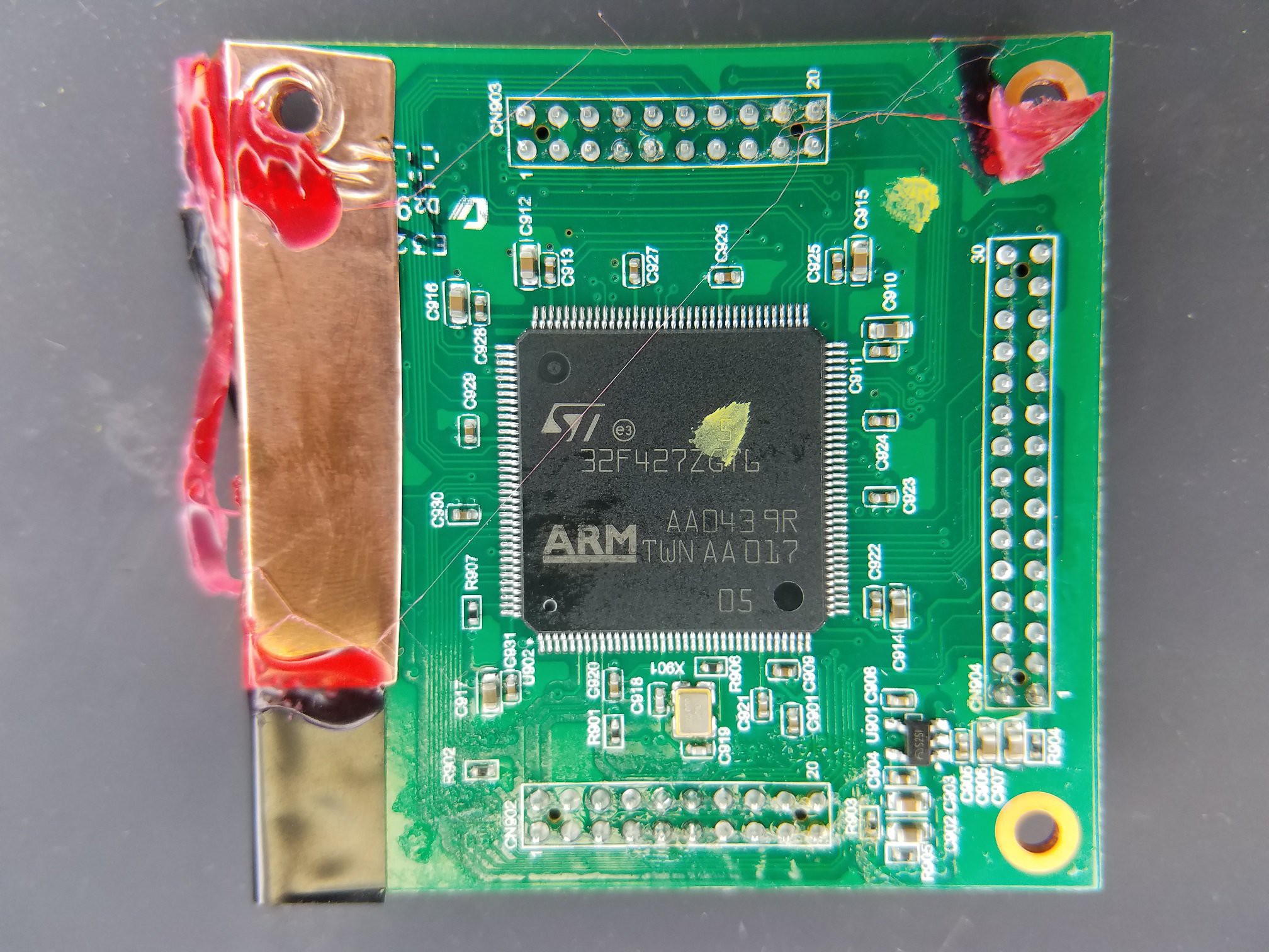
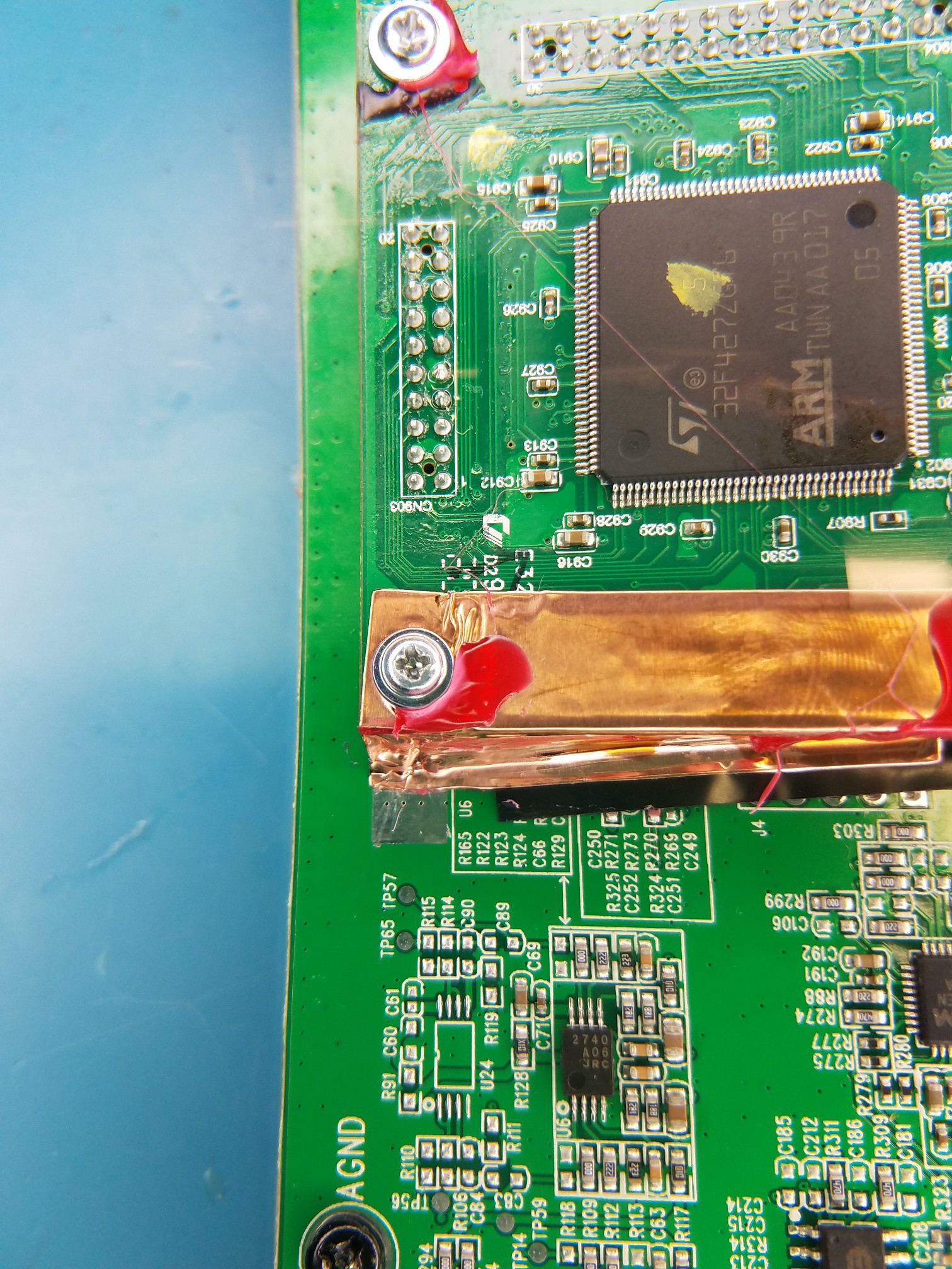
The Spark 40 uses the STM32F427 as the main CPU of this amp. The processor is mounted on a 'removable' pcb module, using standard .050" (1.27mm) M/F headers for the ease of removing the module from the main PCB.
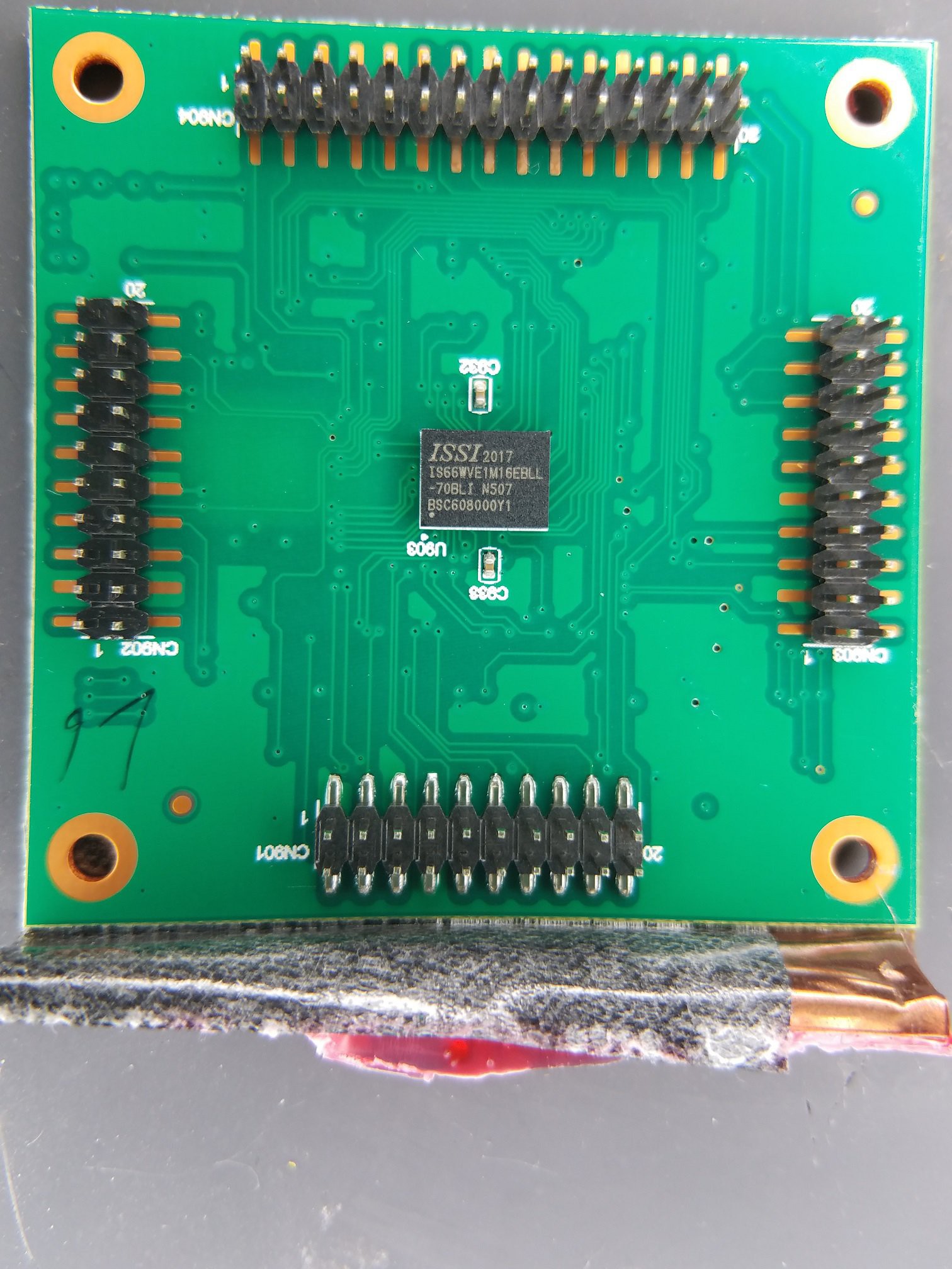
On the underside of the processor module is the ISSI 16Mbit (2MB) SRAM, added on for extra external SRAM to the CPU, since the STM32F4 really doesn't have much internal SRAM.
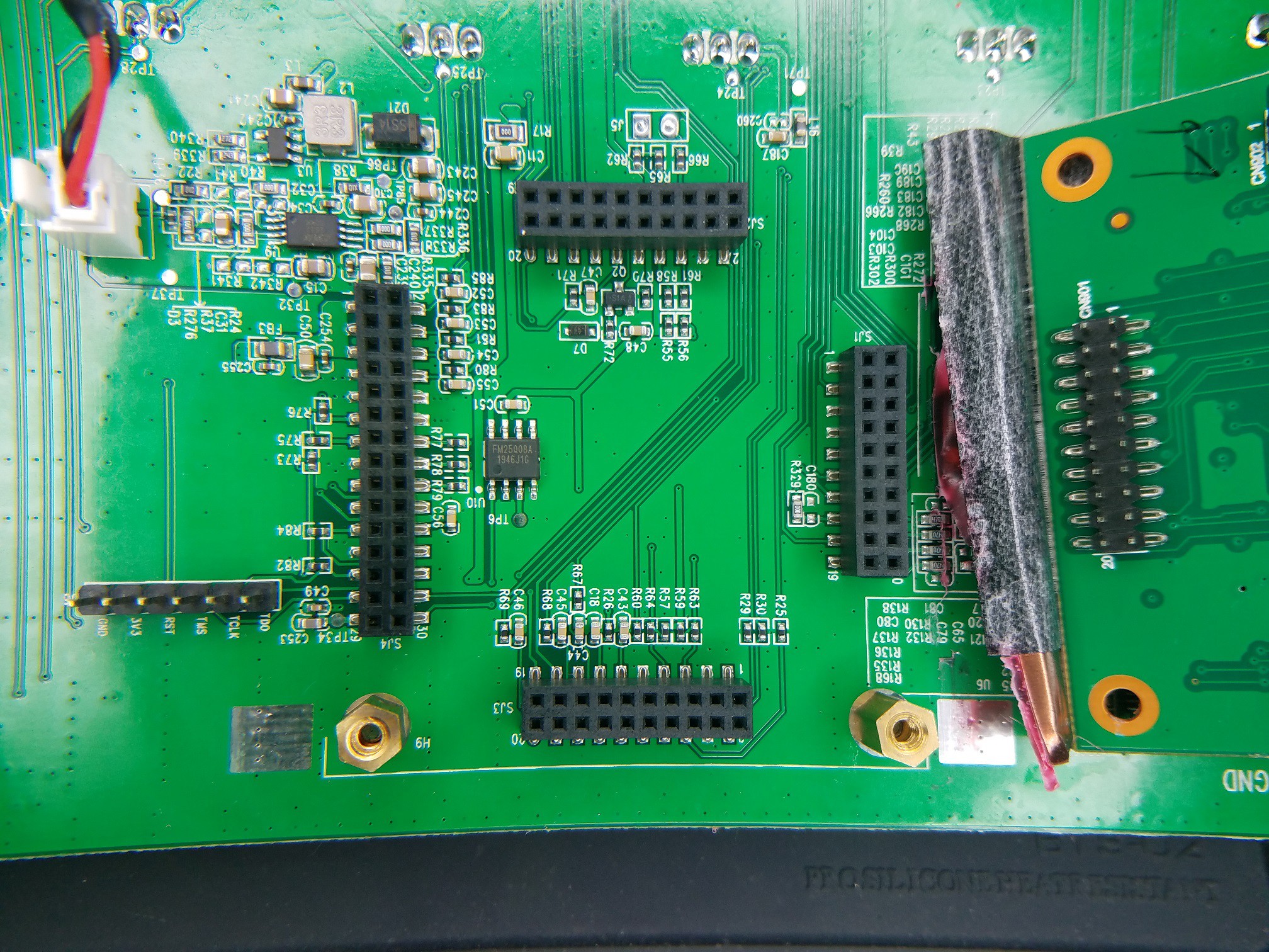
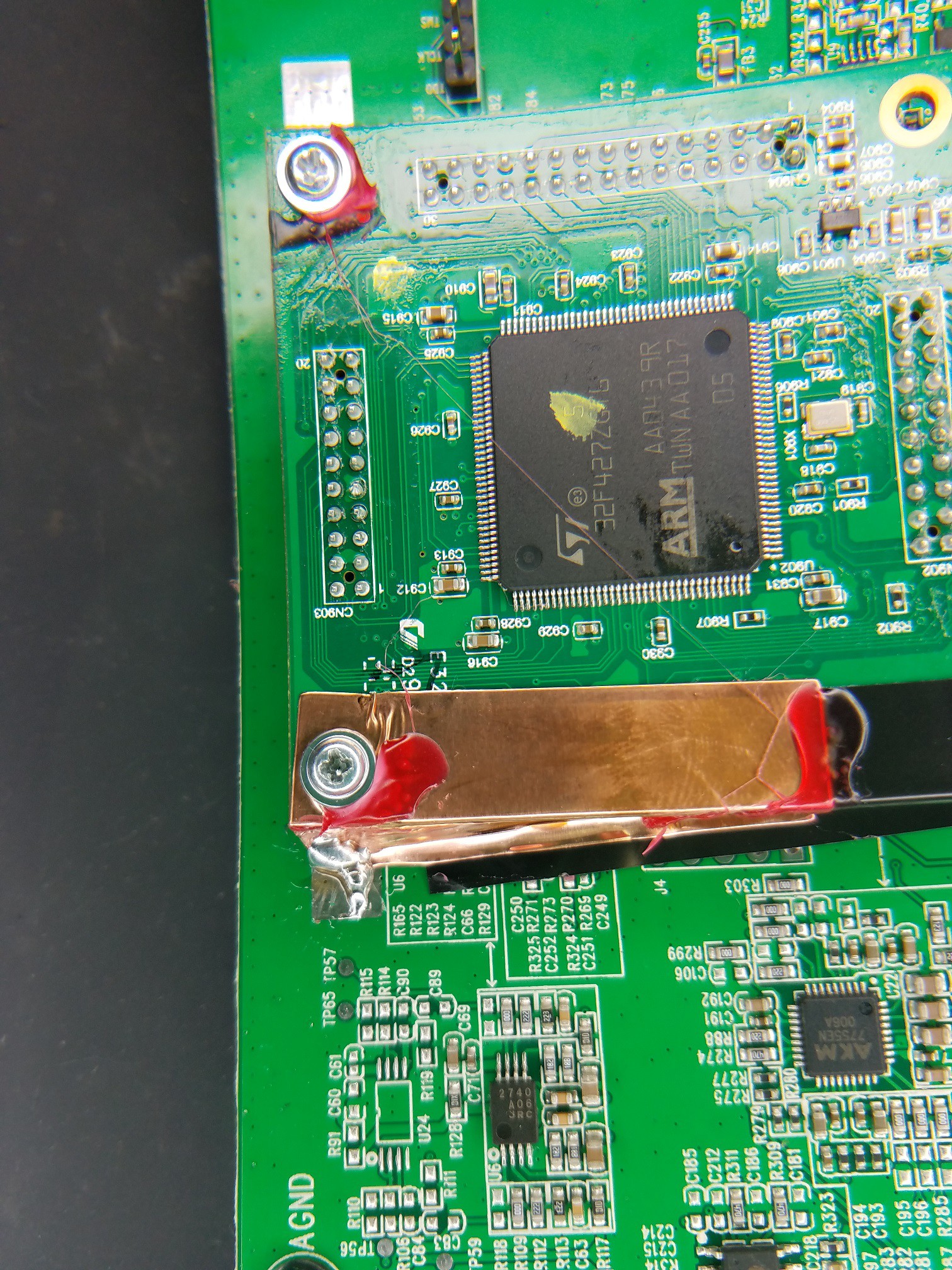
Underneath the processor module on the main board is not much at all, some passive components, and one IC, the FM25Q08A 'Serial 8Mbit (1MB) Flash'. Not sure what exactly they are storing in here... maybe the 4 profiles on the amp, not entirely sure....
You can actually use the processor's 'flash program area' to also store things that the program can use (ie like the profiles), but you also have to be careful to not overwrite this when updating the firmware itself.
So they may have found it easier to just hang a serial flash off of one of the SPI/I2c interfaces on this chip, as the STM32 family has plenty of these.
The processor module also has an interesting piece of copper strip, looks like they wanted to use it as some extra grounding between the processor module and the main PCB? But I'm sure they added GND pins through the headers, so not sure why they added this... Also it wasn't really connected to the GND pad that it was touching, only through some contact glue..
But I added some actual solder between them to make a real connection :)
Discussions
Become a Hackaday.io Member
Create an account to leave a comment. Already have an account? Log In.
LINE OUTPUT for Spark Amp 40 | soulmaster27 | Hackaday.io
Are you sure? yes | no