Just finished building, programming, and testing V3.
Here's some photos.
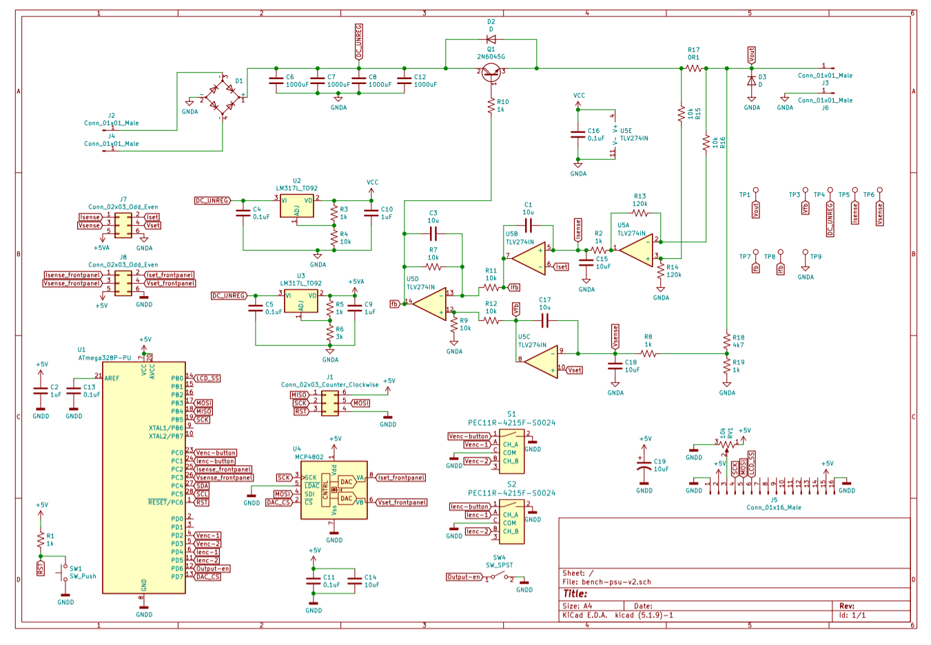
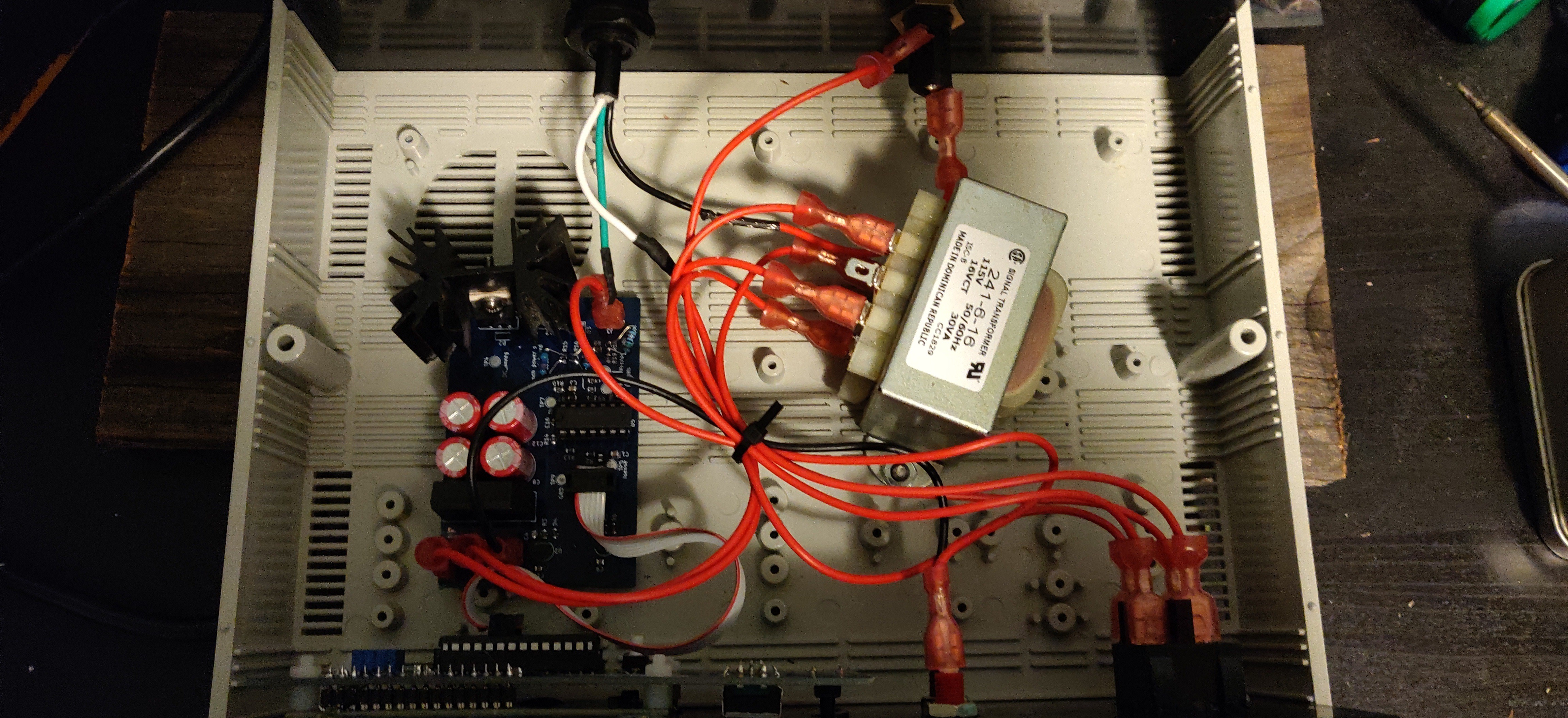
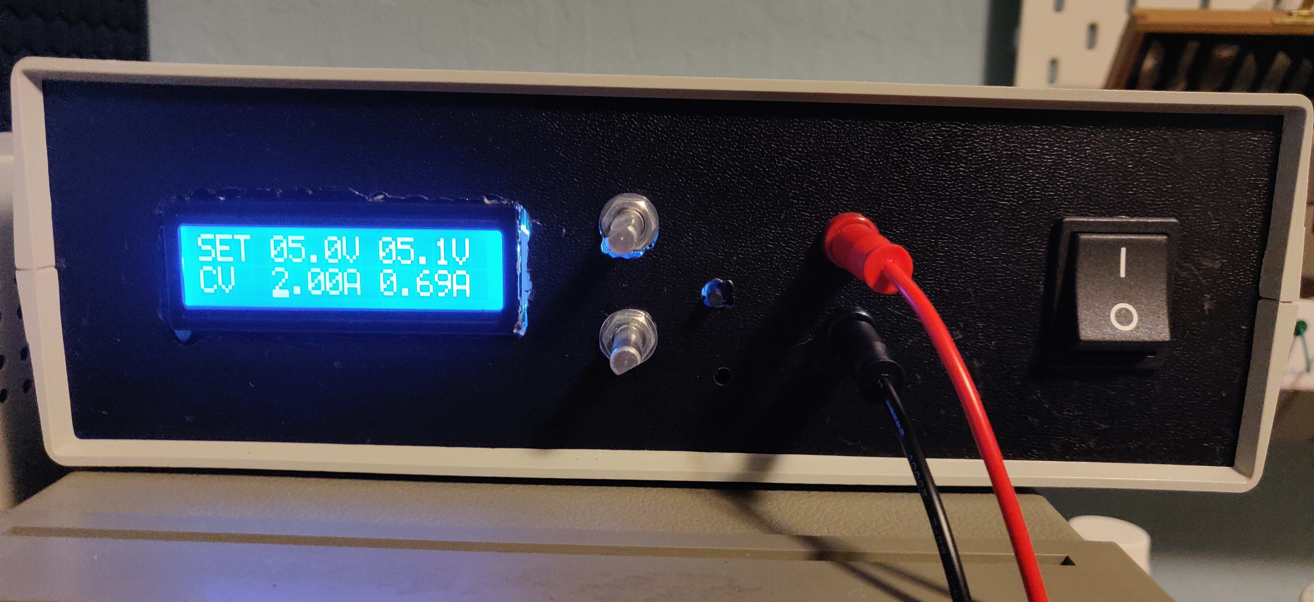
Lots of lessons learned with this project. The schematic does not represent the final design. The biggest change is changing the feedback to be at 1.1v maximum for current and voltage. This was done to use the internal 1.1v reference of the atmega328, instead of the 5v rail. Additionally, I switched from a mcp4802 8-bit DAC for voltage/current setting and moved to a 12 bit equivalent.
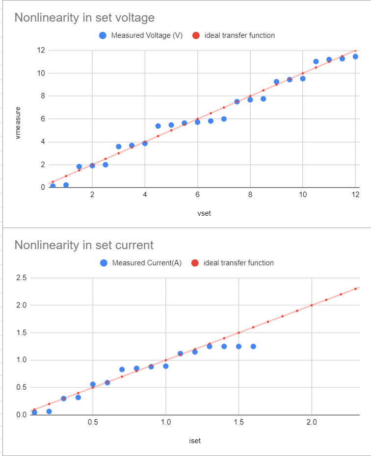
as you can see, with the 8 bit DAC I was getting some pretty horrible differential nonlinearity. After moving to the new DAC, I was also able to quantify some pretty horrible gain offset.
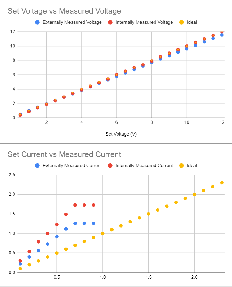
I was able to fix this using linear regression and applying a calibration.
Overall, the biggest lesson I learned was the use of connectors and secure mounting. In previous projects, I soldered everything point to point and hot-glued everything down. Needless to say this was not great. In this project, I used quick disconnected and connected the front board to the mainboard with an IDC connector and ribbon cable. This greatly aided troubleshooting and assembly. (there is however still hot glue... what can I say...)
I'm really stretching the limits of the ATMEGA328 with this project: two encoders, SPI LCD, floating point math.
Discussions
Become a Hackaday.io Member
Create an account to leave a comment. Already have an account? Log In.