I'll start with the data bus since it's 16-bit wide and this is the maximum number of lines that the Analog Discover 2 can handle.
As usual, here's what it is shown during the bootup:
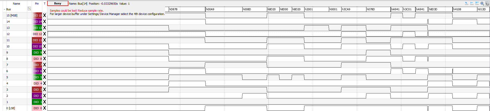
There are a few issues there:
- Not sure whether the ROM pinout is the one that is shown in the earlier log. There are risks of reading the wrong bit or reading the wrong address lines. However, from that website http://www.retrobits.es/2015/08/28/dduc-tuneando-la-mierdaconsola-8bit-que-regalo-abc/, it seems that this ROM pinout is actually compatible to the ST's M59PW1282.
- No CLK line that can be extended for my use on this one. Sadly, the only CLK line is on the 21.47MHz crystal on that board. It can get difficult to see which instruction is actually executed.
- Measuring between the values shown on the bus provided gives timings that are multiples of 1.79MHz CLK periods (approx 558.66nS). Highly suspecting that the CPU is really running on 1.79MHz.
- On a check of a basic 6502 system - the data bus is 8-bit. It is not known how this particular 6502 (or derivative??) can have a 16-bit bus. These clones of NES are very well known to have retrofitted 6502s with extra peripherals. Here, the difficulties of understanding the system increases because it is not understood how it fetches the instructions. Is it most significant byte first? Or the least?
In the meantime I'm going to look into these instructions that are sniffed out and see if they actually make sense or not.
Discussions
Become a Hackaday.io Member
Create an account to leave a comment. Already have an account? Log In.