 strange.rand
The main info here that the new schematic works as expected and the node's deep sleep power consumption is around 5 uA. Also, I successfully tested cold start (charging supercapacitor from 0V), it looks like this
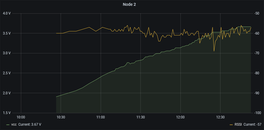
One more image to understand the weather conditions when Vcc reached 2.5V (there was no fog when Vcc reached its maximum, but still cloudy)

Here is the schematic for over/under voltage protection
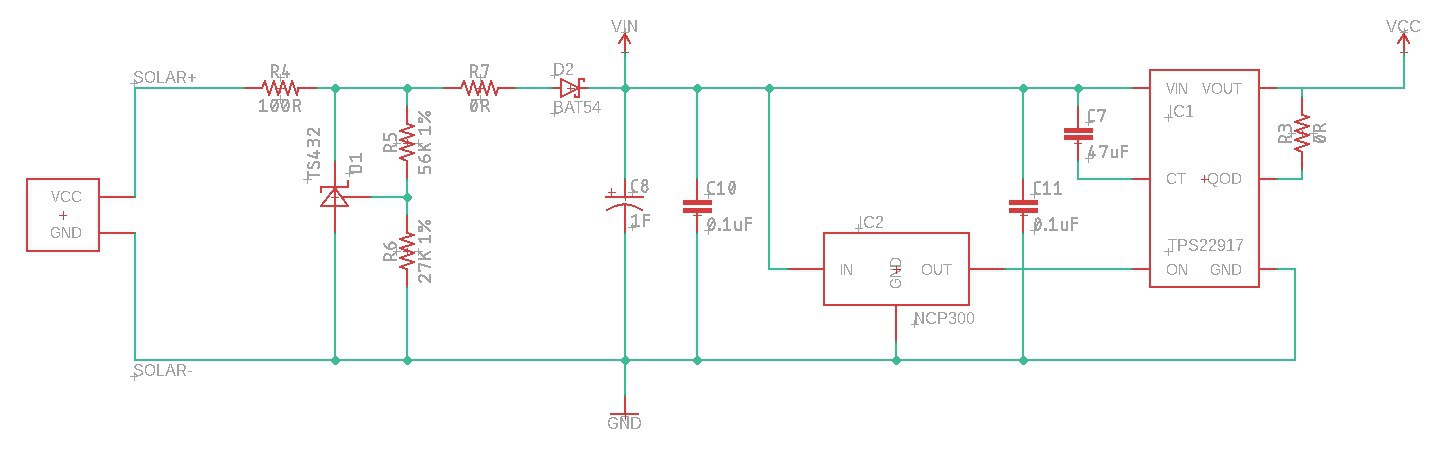 R7 shouldn't be 0R, in the previous experiments I used 100R. The VCC line goes to the MCU and sensors.
As you can see, I've cheated a bit and used a separate IC for switching off the MCU and sensors. Why? There were a few options:
- Low side MOSFET switch
- High side MOSFET switch
- Separate IC
The low side switch is the easiest way to go, but it isn't recommended for switching off MCUs (though, I still think that it might be used in this case).
The high side switch requires a BJT transistor + MOSFET or two MOSFETs and a pull-up resistor. I wasn't sure that using this approach I'll get the required low power consumption, even 1M pull-up causes ~3.6 uA of losses.
The separate IC (TPS22917) advertises operating voltage range from 1V to 5.5V, 2A maximum continuous current (not relevant for this project), and ultra-low power consumption: ON state - 0.5uA, OFF state - 10nA. The IC costs $0.43 on the mouser.
Also, I've ordered separate test PCBs to experiment with the low/high side MOSFET switch, but it'll be later.
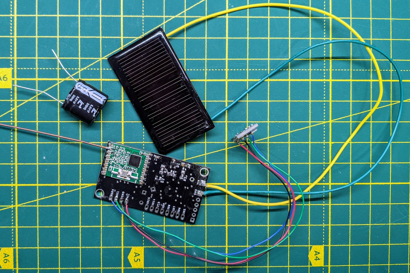
Instead of using a separate low ESR capacitor, as I planned before, I ordered a 1F low ESR supercap (the smallest one, physically). Using it, I do not see any significant voltage drop during the transmission. The smallest low ESR supercapacitor that I able to source locally is 15F 2.7V 12.5*27mm (the price is around $1). It's too big, I'll search on aliexpress for something interesting.
Next steps
- Redesign the PCB one more time (get rid of low ESR capacitor, do not expect "RTC type" supercapacitor)
- Test different sensors
- Design housing for the PCB and sensors
- Create a proper gateway (a separate project probably)
Discussions
Become a Hackaday.io Member
Create an account to leave a comment. Already have an account? Log In.