I wanted to do some projects with a FPGA. Starting out was a little rough, so here are my steps to help you save time.
1) Get the hardware
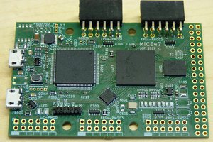
I got the Max10 evaluation board. What I didn't realize when I ordered the board is that the USB cable is for powering the board only. There is no programmer. The board has a power supply, clock, some LEDs and breakout of the pins.
I got the USB blaster, the cheaper version from Terasic. This lets you program the FPGA.
I had an ATMEGA256RFR2 evaluation board. This board runs the controller at 3.3V, so it is compatible with the Max10 evaluation board. This board is nice because you can program the ATMEGA256RFR2 over usb, and also shows up as a COM port, so you can communicate with the microprocessor from a PC.
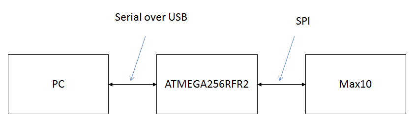
Here is the block diagram. The PC connects to the ATMEGA256RFR2 by serial port (serial over USB), and then the ATMEGA256RFR2 will connect to the Max10 FPGA using SPI.
2) Write the software
For the ATMEGA256RFR2, I wrote a program that lets you use the microprocessor from a command-line like perspective. I'll put the code in a post, but the main idea is that from the PC, you can just read/write the registers of the ATMEGA256RFR2. I wrote and programmed the ATMEGA256RFR2 using Atmel Studio 7.0.
For the Max10, you need to install Quartus (Quartus Prime 20.1) Lite Edition. Once you have it installed, you need to create a new, blank project for the target FPGA. In my case, you need to read the part number off of the chip, 10M08SAE144C8G. I'll post the verilog in a post.
3) Run and test
I connect to the ATMEGA256RFR2 using Tera term. Then, I send bytes over SPI using the sequence of register read and writes. The FPGA responds with a simple byte response.
 Anders Hjelm
 CanHobby.ca
 Stefan-Xp
If you want - check out the next step which was to create a register map and PWM outputs.
https://hackaday.io/project/175677-super-custom-pwm-fpga