 zpekic
Problem statement
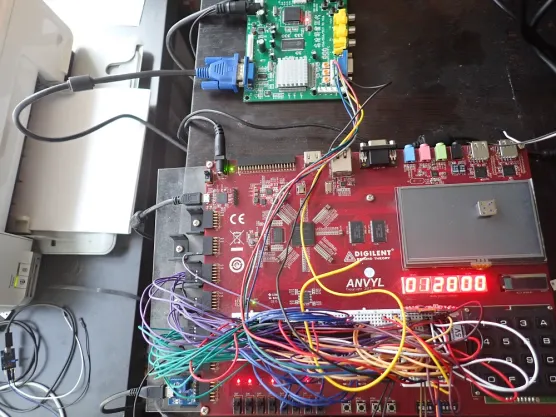
An international group of retro-computing enthusiasts came together to recreate the original TIM-011 hardware (details here), at which point the TIM-011 original video circuit became a focus of interest too. There are two main problems with TIM-011 video:
- Non-standard timing of HSYNC and VSYNC signals, which confuse lots of digital input monitors even if they could take the 16kHz video signal otherwise
- No physically compatible connection with any known connector - just 5 pins poking out from the PCB
In original TIM-011, none of the above was a problem, because a special "paired" monitor was used.
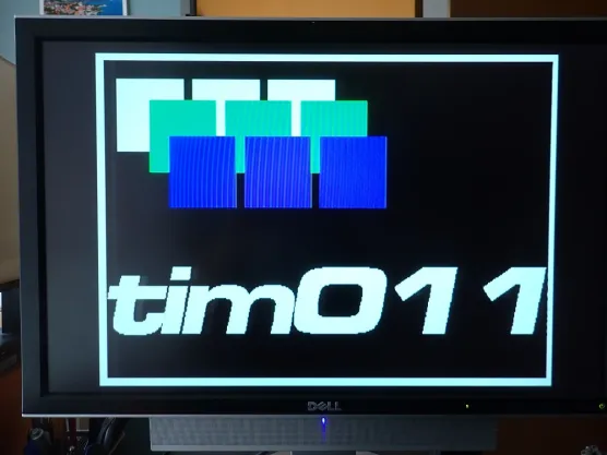
Looking at the details of TIM-011 video circuits, it dawned on me that with some extra logic on the PCB, standard 640*480 VGA signal could be generated - in addition to the TIM-011 video, but not at the same time. This project log is a description how it could be done - not only for TIM-011, but maybe for "home brew" computers, as the video circuitry is extremely "vanilla" and requires only basic 74xx ICs and few passive components.
Video signal summary
Regardless of the video format, a same set of signals is needed, but their frequency and timing must be different. Table below summarizes the signals and their values. Uxx refers to "virtual IC" in the FPGA implementation in VHDL.
| Signal name (or key value) | TIM-011 | VGA | Notes |
|---|---|---|---|
| MODE | 0 | 1 | External signal (generated by software, or hardware switch or jumper) to select which video signals should be generated |
| PIXCLK (HCLK) | 12MHz | 24 or 25MHz | It is also the "horizontal" pixel dot frequency. 50% duty cycle |
| HRESET | 768 | 800 | Single pulse 1 PIXCLK long is generated at this count, determining the length of horizontal scan line. Resets U13A (horizontal scan counter) |
| HS | 576 ... 639 active high | 0 ... 95 active low | Horizontal sync signal timing is critical for CRTs to recognize and adjust to video signal. @msolajic provided updated TIM-011 values, while VGA ones are well known standard values. |
| HBLANK | 512 ... 768 | 0 ... 255 and 768 ... 800 | Horizontal blanking signal (active high) keeps the horizontal pixel counter (U13A) at 0, while at the same time "masking" the V1 and V2 digital video outputs. |
| VCLK | HS f = 15.635kHz | /HS f = 31.25kHz | Because vertical scan and pixel counters are implemented using 74HC4040 which are clocked on falling edge, in case of active low HS for VGA, it has to be inverted. Scan frequency is PIXCLK / HRESET |
| VRESET | 320 | 525 | Single pulse 1 VCLK long is generated at this count, determining the length of the (non-interlaced) frame. Resets U3A (vertical scan counter) |
| VS | 280 ... 319 f = 49Hz | 0 ... 3 f = 60Hz | Vertical sync signal - during this time CPU can read/write VRAM or update the scroll offset register. Frame frequency is VCLK / VRESET |
| VBLANK | 256 ... 320 | 0 ... 127 and 384 ... 525 | Vertical blanking signal (active high) keeps the vertical scan line counter (U3A) at 0, while at the same time "masking" the V1 and V2 digital video outputs. Keeps U3 (vertical pixel counter) at 0. |
| Horizontal pixel range | 0 ... 511 | 0 ... 511 | bits 1 and 0 select 1 out of 4 pixels in the byte, giving 128 bytes (7 bits) in the VRAM address schema: 1HHHHHHHvvvvvvvv (MSB is 1 because 32k VRAM I/O space is visible to CPU from 0x8000-0xFFFF |
| Vertical pixel range | 0 ... 255 | 0 ... 255 | Vertical pixel counter is mapped to lowest 8-bits of the address. This allows easy hardware vertical scroll by adding to this value an 8-bit offset. 1hhhhhhhVVVVVVVV |
Analyzing the signal comparison table above, one possible hardware solution becomes apparent:
- Introduce a 8-bit wide 2 to 1 MUX to select the signals above, and the selection is the MODE signal
- Keep the existing horizontal and vertical pixel counters (U13 and U3) as the VRAM addressing does not depend on the MODE, but use them only for that, not any other signal generation. So U13 and U3 always cover only 512*256
- Introduce 2 additional 74HC4040 counters (U13A and U3A) which cover either 800*525 or 768*320 depending on MODE, and use these to generate all the HS, VS, HBLANK, VBLANK, HRESET an VRESET signals.
- To simplify signal generation, two 3-to-8 74x138 decoders (U13B and U3B) are driven by U13A and U3A - these allow "slicing" horizontal and vertical pixel counts by 128 increments.
- All other parts of video circuit remain unchanged, such as V1 and V2 generation, scroll register, latching VRAM data byte at read or write etc.
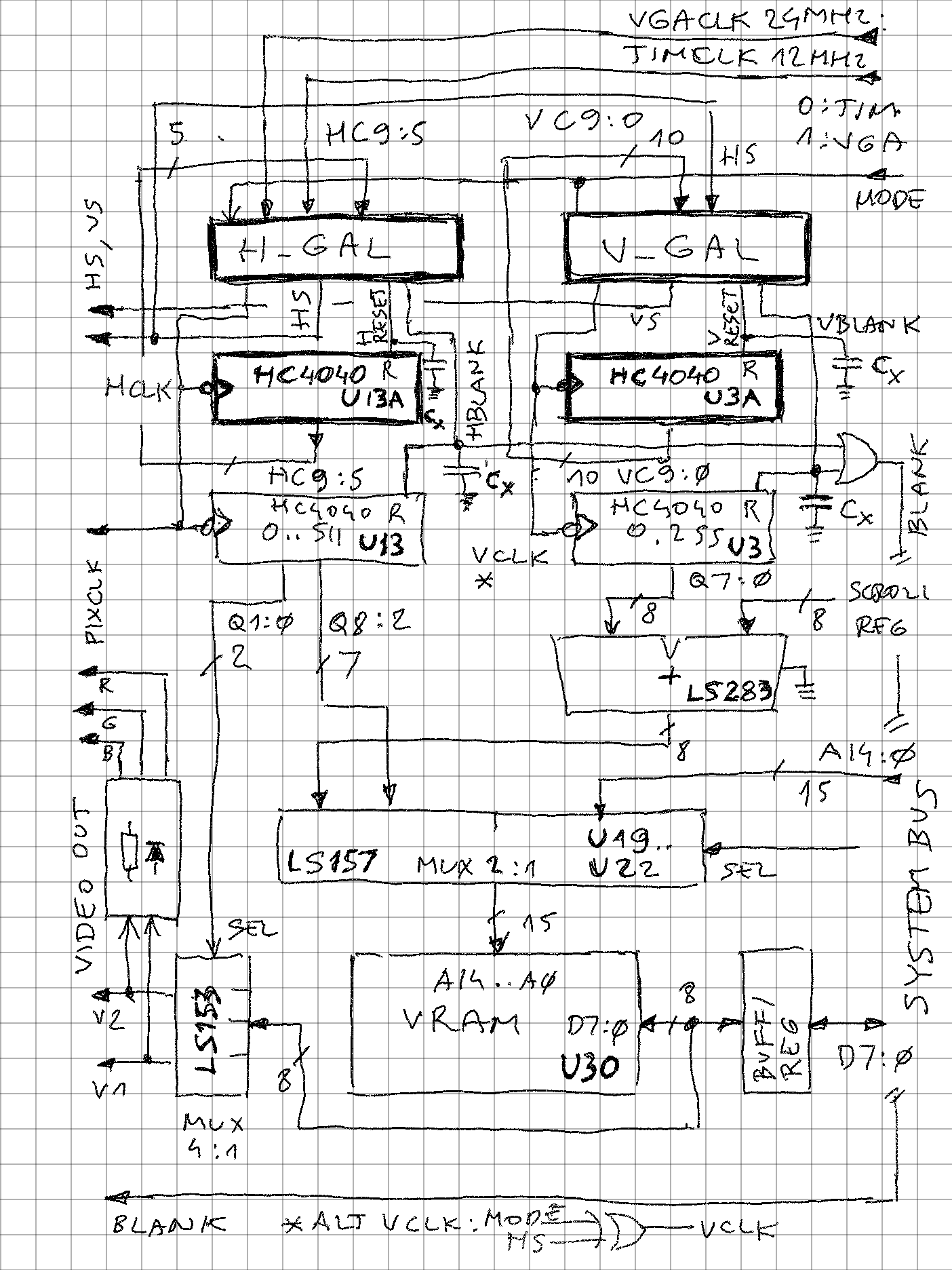
Dual-mode video high-level schematic. Bold border ICs are additions to original TIM video (rest of circuit is unchanged)
TIM-011 mode
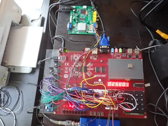
As I didn't have legacy CRT at hand (for example Sony CPD-1302) I used the Gonbes GBS-8200 to convert 4 signals to VGA (code from top-level VHDL component):
-- Connect to GBS8200 gray wire (composite sync!)
    gr_csync <= gr_hsync xor (not gr_vsync);
    GBS8200_GRAY <= gr_csync when (sw_mode = '0') else '0'; --gr_hsync xor (not gr_vsync);

-- connect to GBS8200 blue / green / red wires
-- colors: black, blue, green, white
    GBS8200_BLUE <= gr_vid1 when (sw_mode = '0') else '0';
    GBS8200_GREEN <= gr_vid2 when (sw_mode = '0') else '0';
    GBS8200_RED <= (gr_vid1 and gr_vid2) when (sw_mode = '0') else '0';
Some notes:
- Output signals are kept permanent 0 in VGA mode (to prevent higher frequency VGA signals driving the lower bandwidth video output)
- GBS-8200 takes composite sync, not 2 independent HS and VS signals, so they are simply combined using XOR
- RGB digital video allows for 8 colors, but TIM-011 only generates 4 levels (each pixel takes 2 bits, 1 VRAM byte = 4 pixels). In other words, any 4-entry "palette" out of 8 possible colors can be obtained. In the very simple scheme from the code above, colors will be:
- 000 - black (V1 and V2 both off)
- 010 - green
- 001 - blue
- 111 - white (V1 and V2 both on)
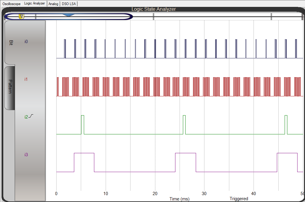
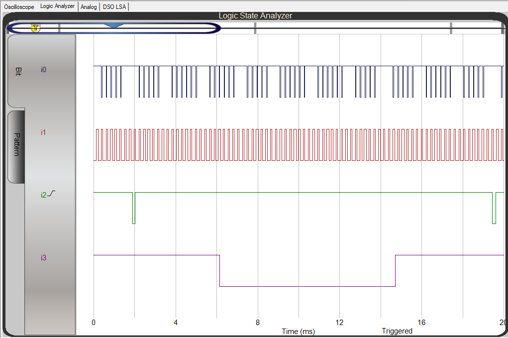
TIM mode HS(ync) and HBLANK (HSync is positive, duration is 64 dot clocks @12MHz = 5.64us; HBLANK is simultaneously reset signal for horizontal counter U13A)
TIM mode VS(ync) and VBLANK (VSync is positive, VBLANK is simultaneously reset signal for vertical counter U3A )
VGA mode
VGA signal is generated directly from FPGA. Note the 2:1 aspect ratio (as TIM-011 resolution is 512*256 pixels) centered into 640*480 VGA pixel window (margins are "blanked" using the HBLANK and VBLANK signals explained in the table above).
From top-level VHDL component:
-- VGA connections
-- colors: black (000), dark gray (333), light gray (CCC), white (FFF)
    gr_color <= gr_vid2 & gr_vid2 & gr_vid1 & gr_vid1;
    HSYNC_O <= sw_mode and gr_hsync;
    VSYNC_O <= sw_mode and gr_vsync;
    RED_O <= gr_color when (sw_mode = '1') else X"0";
    GREEN_O <= gr_color when (sw_mode = '1') else X"0";
    BLUE_O <= gr_color when (sw_mode = '1') else X"0";
Notes:
- Output signals are kept permanent 0 when in TIM mode (to prevent VGA monitors to "autodetect" in vain)
- This FPGA board can generate 4096-color VGA (each component 4-bit, 16 values), so 4 out of 4096 colors are possible. Simple connection solution in the code above allows generating 4 levels of gray which is close to original TIM-011 approach.
VGA mode HS(ysnc) and HBLANK (HSync is negative polarity, horizontal counter U13A can only count 0..511 when HBLANK is low)
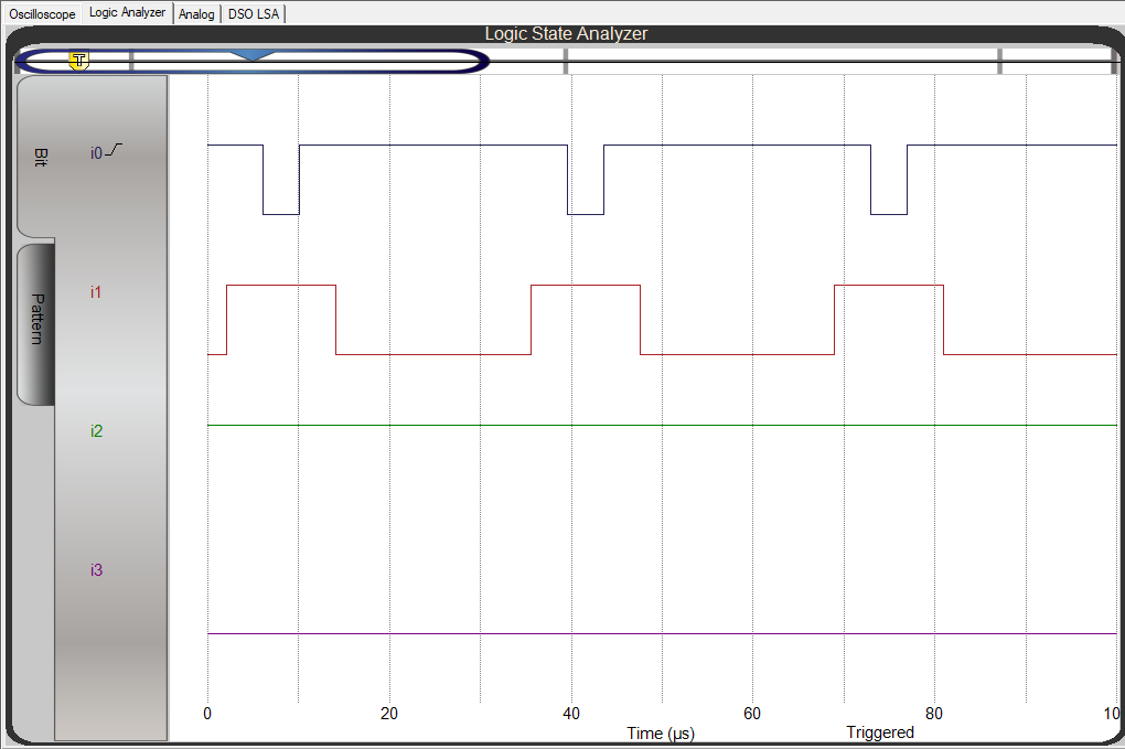
VGA mode VS(ync) and VBLANK (VSync is negative polarity. Vertical counter U3A can count from 0 .. 255 only when VBLANK is low)
Discussions
Become a Hackaday.io Member
Create an account to leave a comment. Already have an account? Log In.