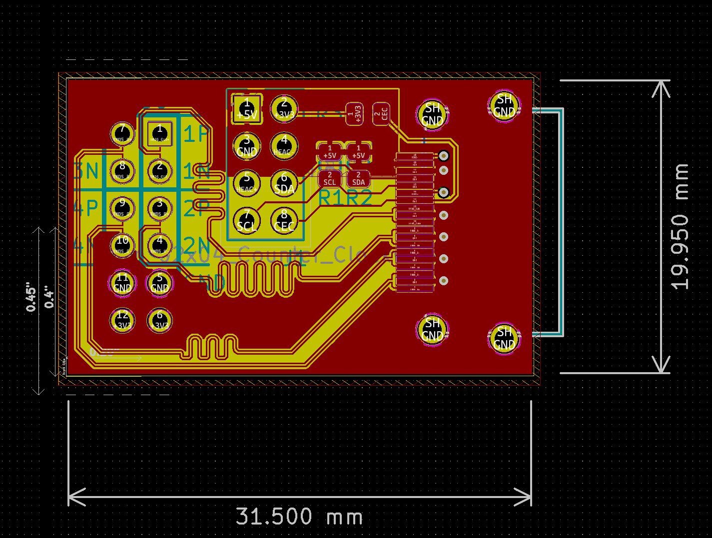
I started doing layout with JLCPCB's 2-layer stackup, but I quickly realized that I wasn't going to be able to hit 100 ohm differential mode characteristic impedance with such a thick dielectric. Lucky for me, JLCPCB offers 4-layer boards for just a couple more dollars. They offer two separate 4 layer stackups: JLC7628 and JLC2313. I went with JLC2313 since the thinner dielectric shrinks your trace width when controlling the impedance.
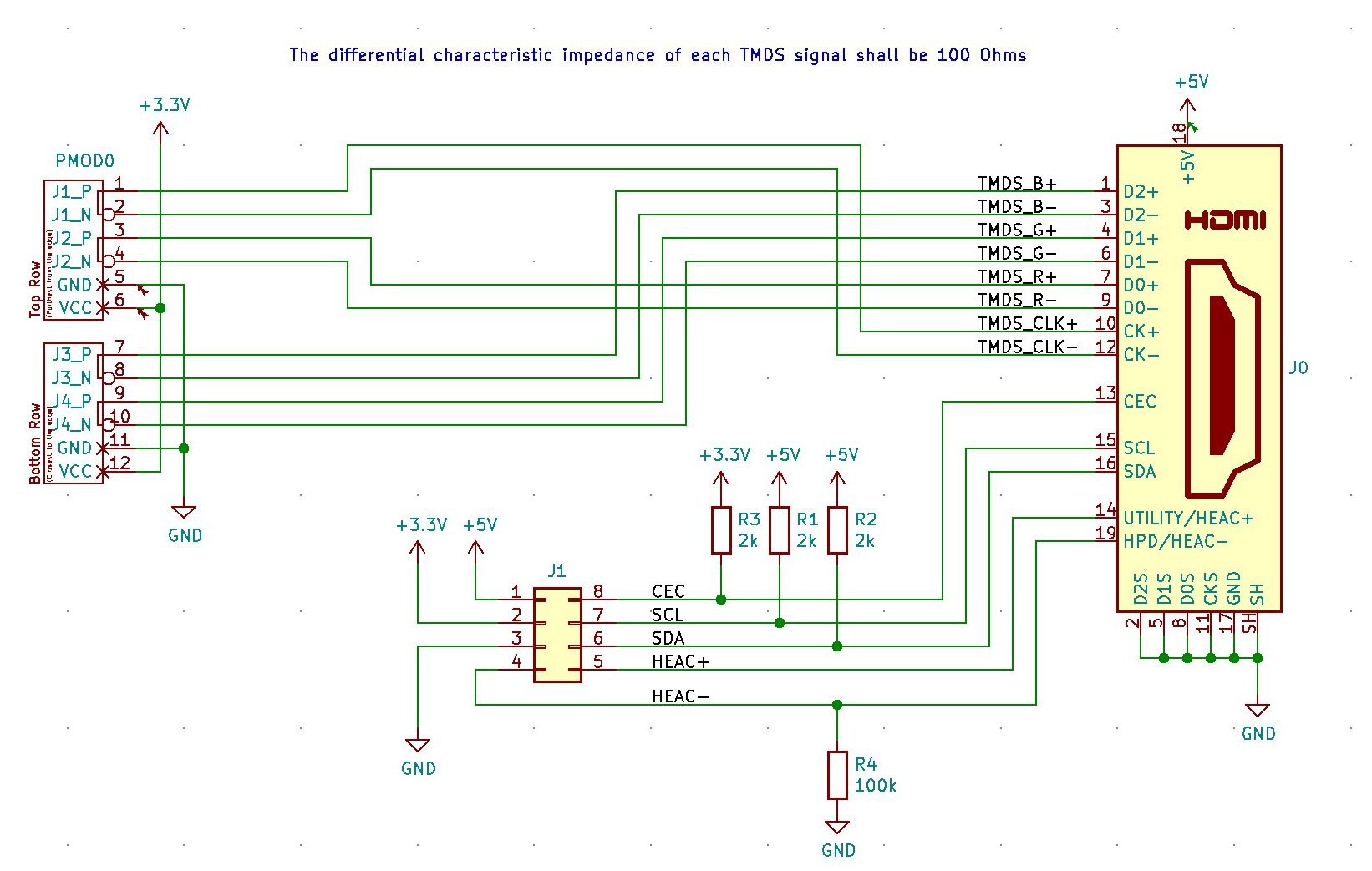
I also made a couple changes to the schematic, including swizzling around the TMDS pairs to make routing easier, and adding in some missing pull-ups and pull-downs.
I have also been playing around with the OpenEMS 3D field solver in my spare time, and I would really like to plug this board into it and see how well it holds up. I used JLCPCB's calculator for choosing track width and spacing, and I am curious how accurate it is. I might potentially create some S-parameters for the board as well, but we'll see.
Discussions
Become a Hackaday.io Member
Create an account to leave a comment. Already have an account? Log In.