Dual Interleaved CS42448 Chip
16 Audio In & 16 Audio Out using only 5 pins
16 Audio In & 16 Audio Out using only 5 pins
To make the experience fit your profile, pick a username and tell us what interests you.
We found and based on your interests.
Created an updated CS42448 board with small improvements and a header to connect to this interleaved TDM experiment.
https://hackaday.io/project/2984-teensy-audio-library/log/187557-updated-cs42448-pcb-for-teensy-4x
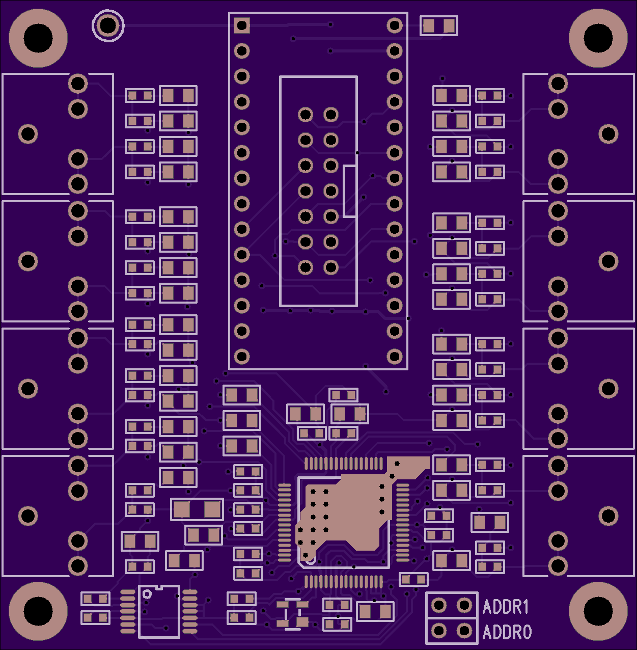
I added a 74LVC74 flip flop chip which will retime the FS2 and MUX control signals to the falling edges.
PCB sent to OSH Park, parts on order from Digikey. Now begins another wait...
https://oshpark.com/shared_projects/KbStFsrm
So what hold time are we supposed to have? I looked it up in the datasheets for the 2 TDM chips I've used so far...
Looks like CS42448 wants 5 ns hold time for data, but 16 ns hold time on the frame sync. Yikes! Looks like I'm going to need to delay the FS pulse to the next falling edge.
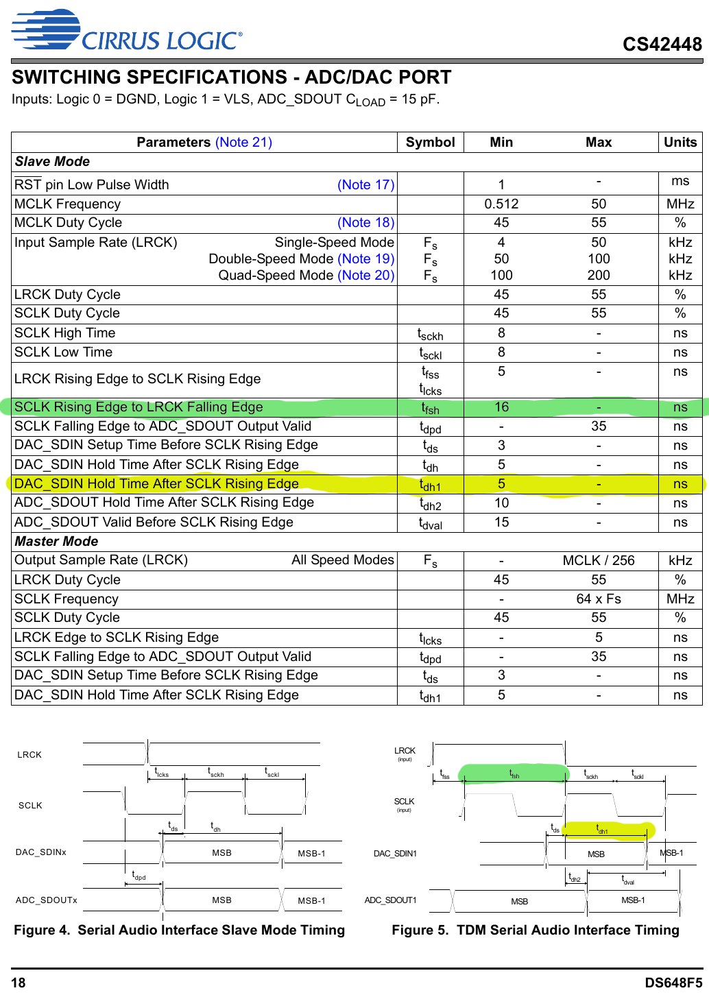
... minor rant: Whoever at Cirrus (maybe then Crystal?) drew this Figure 5 timing diagram really made it confusing by extending the Tdh time all the way to the next rising edge. I'm sure it was convenient (lazy?) and visually appealing not to have a gap between Tdh and Tsckh. But it visually implies LRCK (which I'm calling the frame sync pulse) needs to go longer, even though the spec says only 16ns. Even worse, visually it seems to suggest the end of LRCLK should go to the next rising edge of SCLK. Really wish whoever writes these datasheets would do better!
ADAU1966A seems to be a little easier, wanting 5 ns on both.
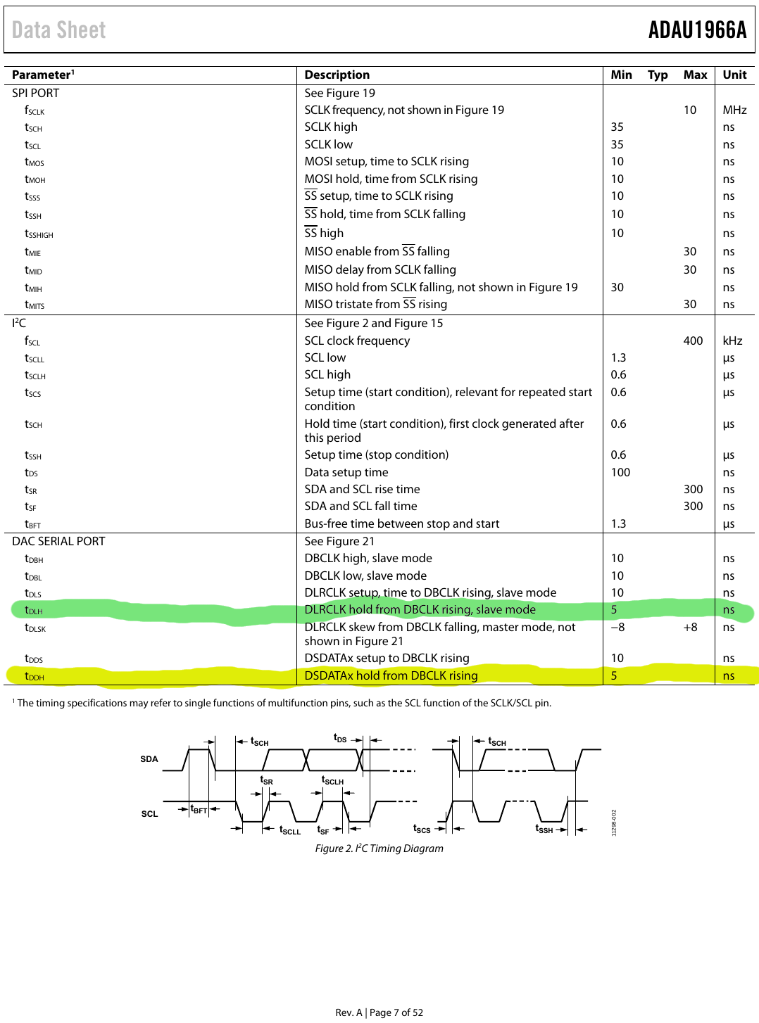
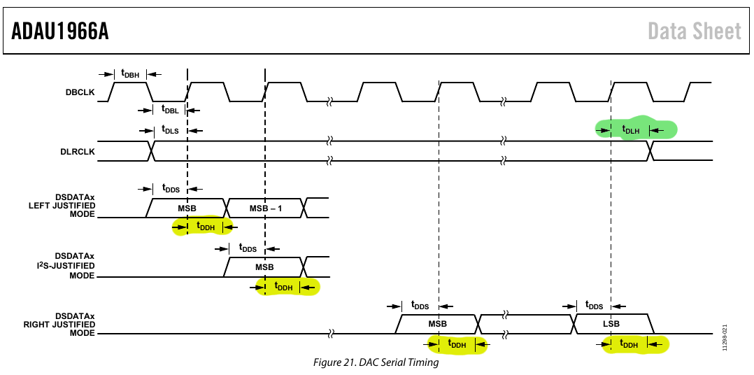 Analog Devices really shows how to compose a good timing diagram. The dotted lines from the clock edges to only the meaningful timing specs really helps communicate which things matter. Nice!
I woke up thinking that I never actually verified the frame sync pulse was really in the correct position in the 256 bit frame. It's not like Verilog or anything else reliable created this circuit... just me doodling NAND & NOR gates on graph paper.
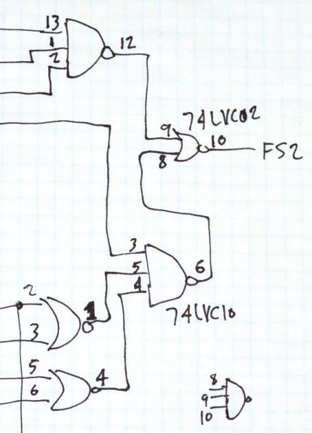
(plus me connecting them right in the PCB layout without any sort of CAD schematic, but as you can see, I did write in the pin numbers on the paper as I chose each gate's pin to use in the layout)
So I loaded the image in Gimp and added text for each rising edge's bit number.
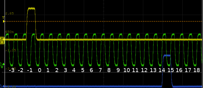
That's a minor relief.
But I'm still a little worried about hold time. I probably need to get out a CS42448 board and look at whether Teensy and the CS42448 are updating their data outputs on the rising or falling edge of BCLK.
Built up 1 of the boards and connected it to my scope for a first look at the waveforms.
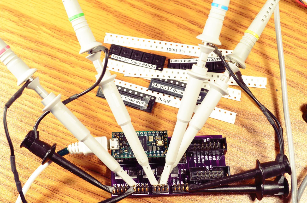
Here's the big picture view, of the entire 256 bit TDM frame. Or two of them, plus edges of 2 more, so ~600 bit times shown here. Thanks to the scope's frequency counter you can see the yellow frame sync pulse is happening at 44.1 kHz. So this view is the time of 2 audio samples, and of course the goal is to pack 16 sets of 16 bit data originating from 2 different CS42448 chips into those 256 bit times!
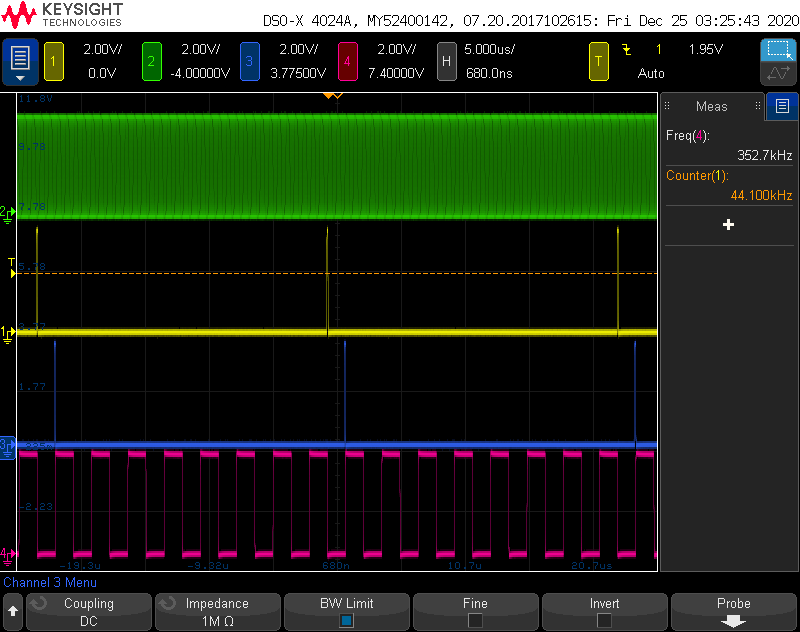
The green and yellow traces are the bit clock and frame sync generated by Teensy 4.0.
Blue is the 16 clock delayed frame sync intended for the 2nd CS42448 chip. Red is the 2:1 mux control signal, which will select which CS42448 chip talks to the Teensy TDM data pins.
Just to recap... the idea is the 2 CS42448 chips are running from the same bit clock, but one is 16 cycles delayed. CS42448 uses 32 bit data, but the low 8 bits are always zero and the next 8 are pretty much always just noise. So the mux routes each chip's 16 most significant (and only worthwhile) bits to Teensy 4 while the other chips (worthless) 16 least significant bits are discarded.
But upon zooming in, I saw something I probably should have considered, but didn't think about until now....
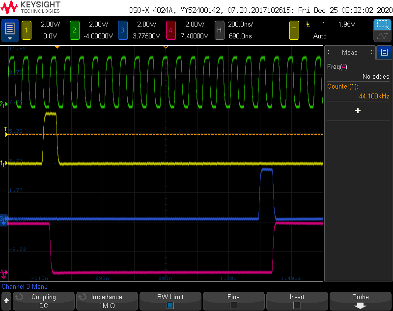
We might have a problem with setup or hold time. Maybe. Here's a view with the bit clock positioned between the 2 frame sync signals, so it's easier to see.
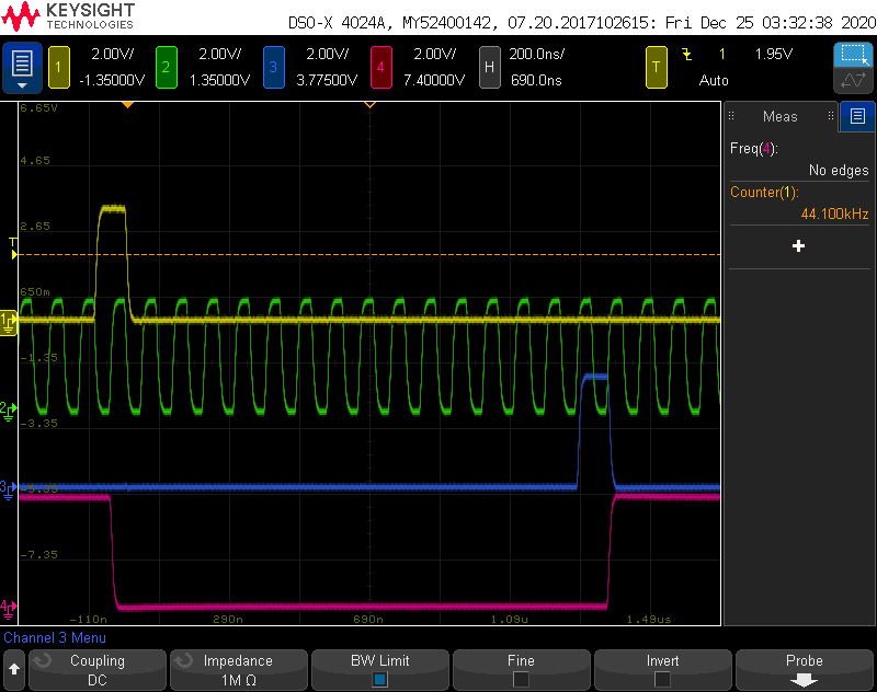
Teensy 4.0 is generating the frame sync pulse on the falling edge of the clock. The CS42448 uses it on the rising edge. So this way gives the best possible timing margin, it's valid half a cycle before needed and remains stable for another half a cycle.
But my little logic circuit is updating it outputs on the rising edge. So a big question is whether the CS42448 needs the signal to remain stable for a hold time after the rising edge?
Here's an intense zoom in...
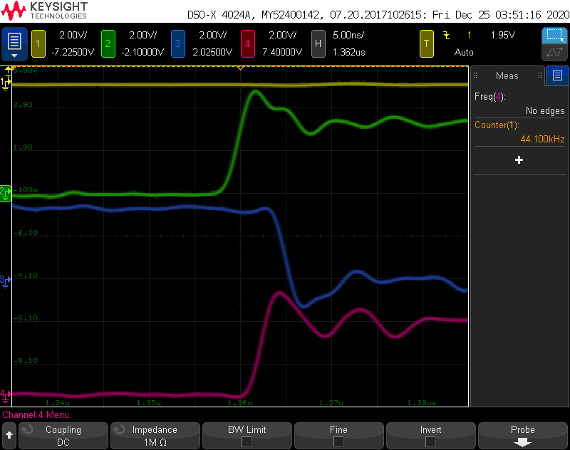
Looks like frame sync (blue) stays valid about 5 ns after the clock edge (green). The mux control changes about 2.5 ns after the clock, but maybe that's ok since the logic inside the mux chip will add a little more delay to the data signal.
In hindsight, maybe I should have used 2 more flip-flops to retime the control signals onto the falling edges?
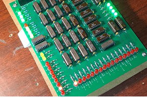
Created a PCB and sent it to OSH Park.
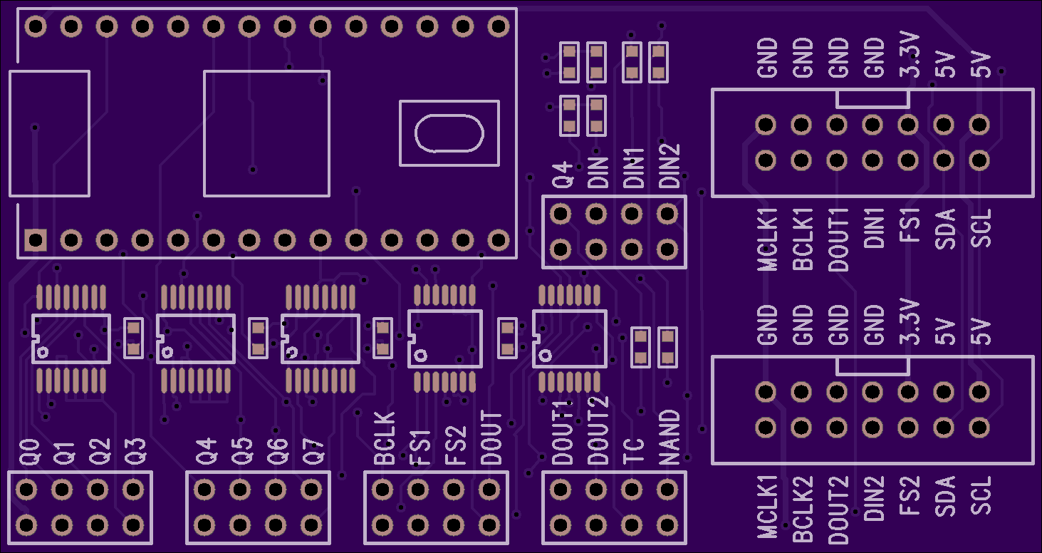
https://oshpark.com/shared_projects/d8YVVeck
As I usually do, just put the footprints right into the layout and quickly clicked to connect the netlist like me scribbled schematic.
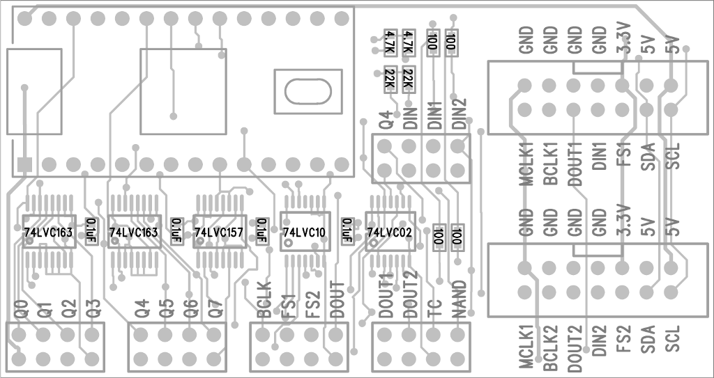
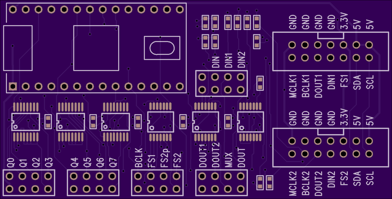
I also brought almost all the signals to 8 pin headers which will mate with a Saleae logic analyzer. Long ago, when I had more time, I probably would have prototyped this on a breadboard or vector board with point-to-point soldering. But that takes a lot of time to build. Took only an hour to quickly connect up all the parts on this PCB.
Of course with a PCB there's a long wait. I also chose postal shipping on a Digikey order for the 74LVC chips. Going to put this all aside until the PCB and parts show up.
In the spirit of trying to share as I go, here's my first idea of how this state machine might work.
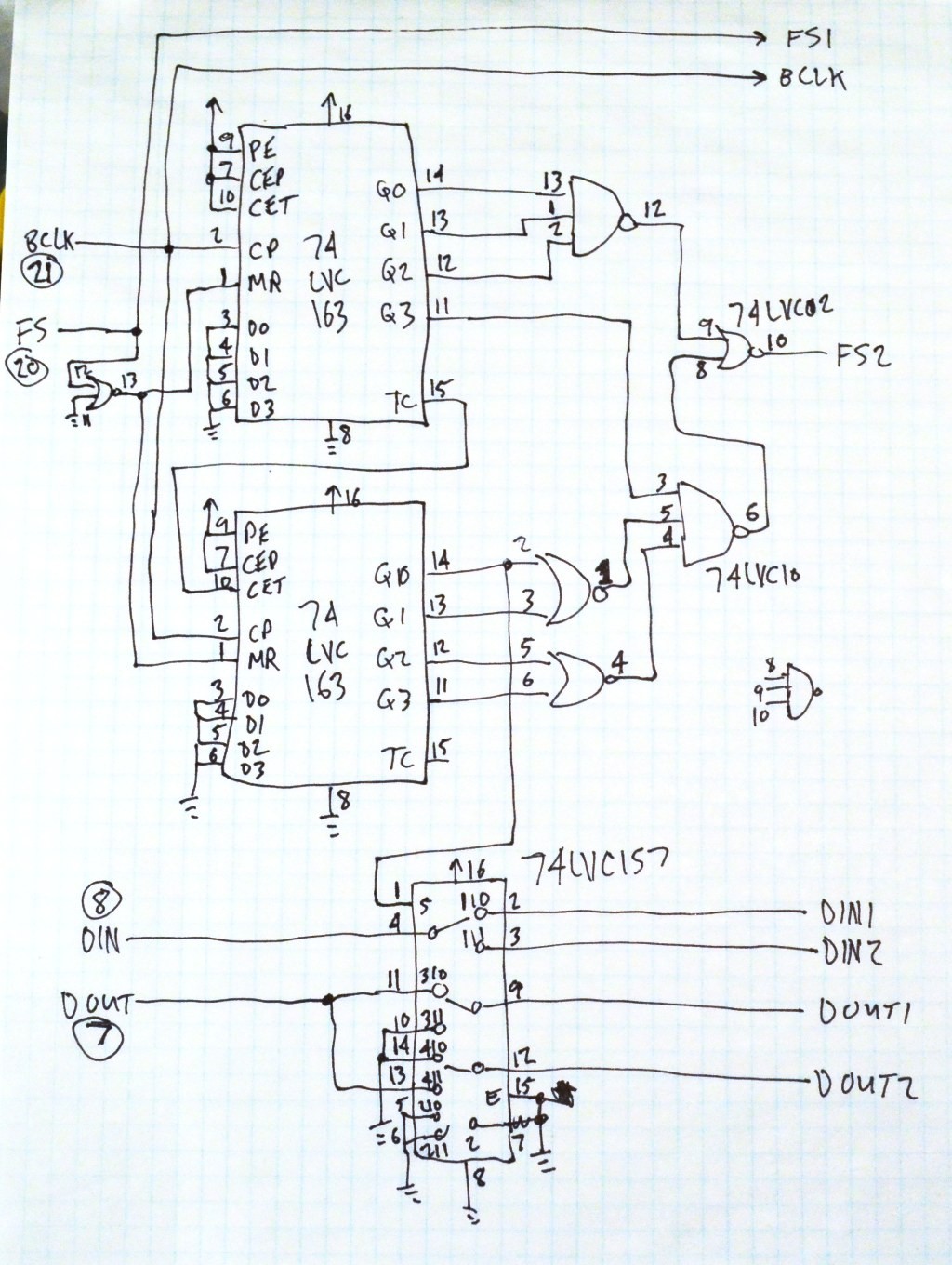
The basic idea is those 74LVC163 chips are connected to form an 8 bit counter, which gets reset when the FS signal is asserted.
The 2:1 mux chip routes the output from one of the CS42448 chips to Teensy every 16 cycles, and it sends Teensy's output alternately to the 2 chips in each 16 cycles.
Those NAND and NOR gates are supposed to generate a logic high when the counter is at 00001111, and logic low for all other states. I didn't simulate or test this at all... just made it up and doodled it on this graph paper. It's completely untested!
Create an account to leave a comment. Already have an account? Log In.
Become a member to follow this project and never miss any updates
By using our website and services, you expressly agree to the placement of our performance, functionality, and advertising cookies. Learn More

 Paul
Paul
 Jac Goudsmit
 Nicolas REIMEN
Very excited to follow this build Paul! Ive tried and failed at designing PCBs around the
CS42448 and CS5368 so i will be following closely.