 Jelto
JeltoThe first challenge was to think about how to arrange the cells. Requirements from my side were:
- Modular/stackable design to extend the powerbank
- Stable and reliable assembly for portable use
- Dedicated fuse for cells for more security
With this requirements I decided against just taping all cells together. A way more appealing approach was to design a custom PCB which houses the cells. This PCB can then be used to stack the cells and also to connect them electrically.
For connecting the PCBs I used M3 spacers. The spacers can either be out of metal for a electrical connection or plastic, to isolate (for future designs when doing 2S or 3S cell design). In both cases the spacers give enough structural enforcement for large modules.
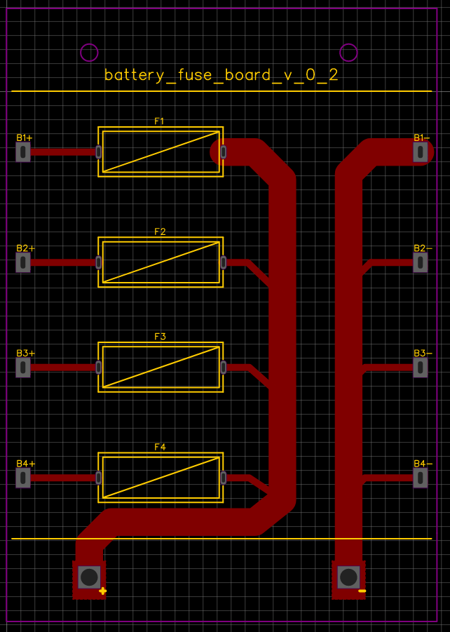
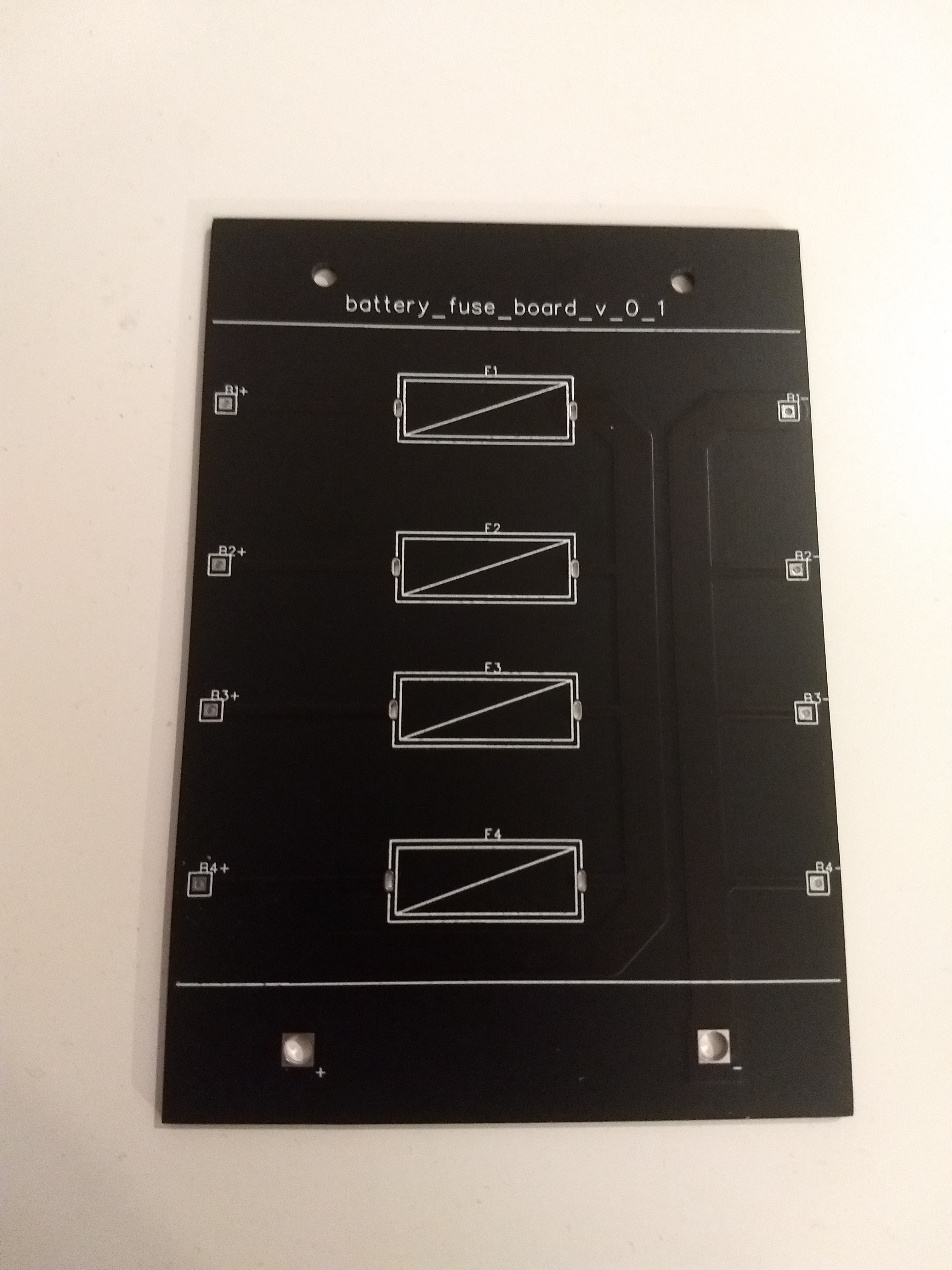
So I started a PCB design software, watched some tutorials and created version 1 of the pcb (v2 in the image):
I ordered the PCB from JLCPC. After 2 weeks 10 PCBs arrived. My first lesson in designing PCBs was: measure twice and doublecheck everything! The holes for the 18650 cell holders were way to small!
However the other components fit to the PCB. I've done a test-fit with the fuse holders and the M3 standoffs:
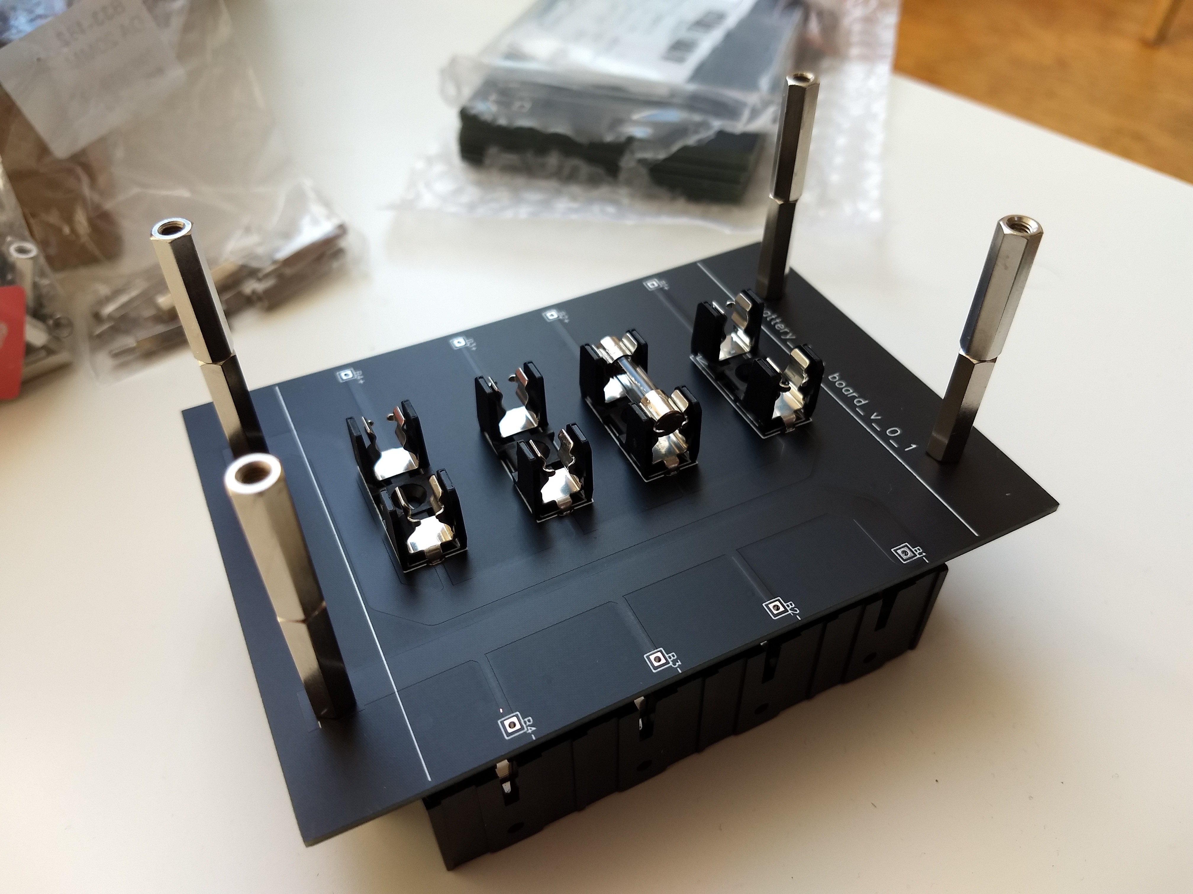
Here you can see quite good the small holes for the cell holders. I tried to increase the hole size using a drill press but that did not work.
Discussions
Become a Hackaday.io Member
Create an account to leave a comment. Already have an account? Log In.