 techknight
Remember the discussion I had earlier? Yeah, that's right. those pesky FPGAs and PALs.
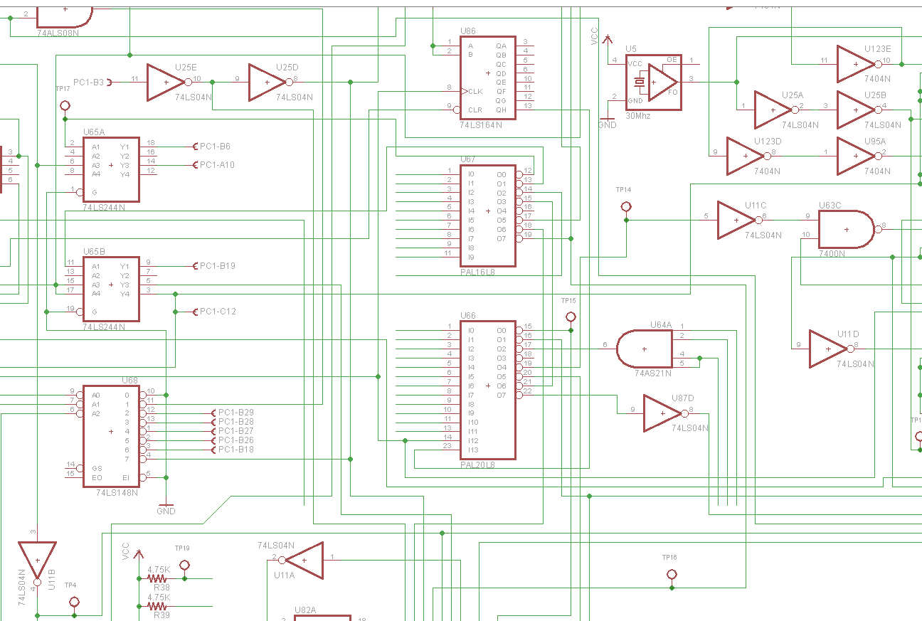
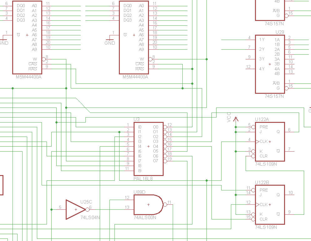
So once we have the schematic drawn out, I can begin to stand back and take a big picture look at this thing and begin to study its design and architecture. However, you see things like this:
Basically, that doesn't really tell you a whole lot. Seems a lot of the logic is locked up inside those PALs. As seen above.
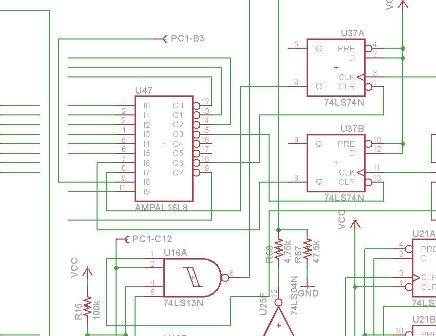
Another one:
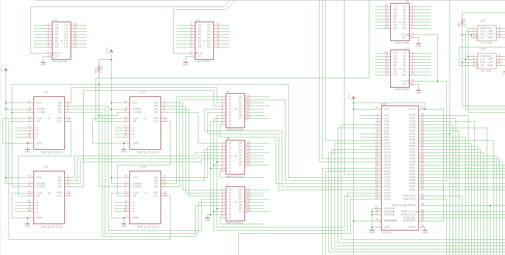
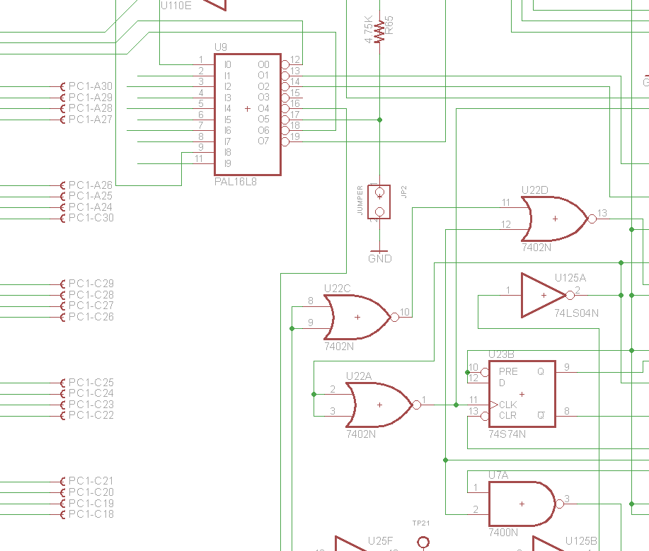
The one I am most afraid of, is yes. the FPGAs and PALs associated therein:
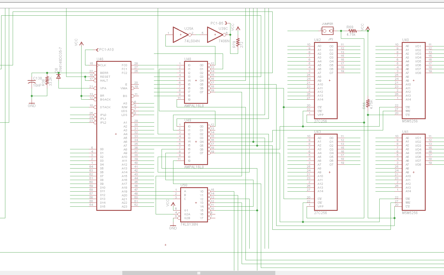
We take a look at the CPU card, and more of the same:
Especially in the Bus/RAM sections:
I suppose using PALs and other logic arrays were not that uncommon in the late 80s, probably to keep cost down or board space usage down. But then again, looking at how this unit was engineered? I don't think cost was an object.
Regardless, There isn't any way around other than figuring out a method to reverse the logic out of the PALs. Luckily? the majority of the PALs are L style, or combinational logic.
There are a couple registered logic PALs on the graphics card, But... those still remain a mystery to this day. They appear to be gating for the pixel clock and a frequency divider for the PLL.
Next step..... figure out those PALs.
Discussions
Become a Hackaday.io Member
Create an account to leave a comment. Already have an account? Log In.