 techknight
Since at this point I have pretty much figured out that I am on my own with this, with the exception of a few good friends for support, I decided to start my journey. Now that the preface is over, its time to move on!
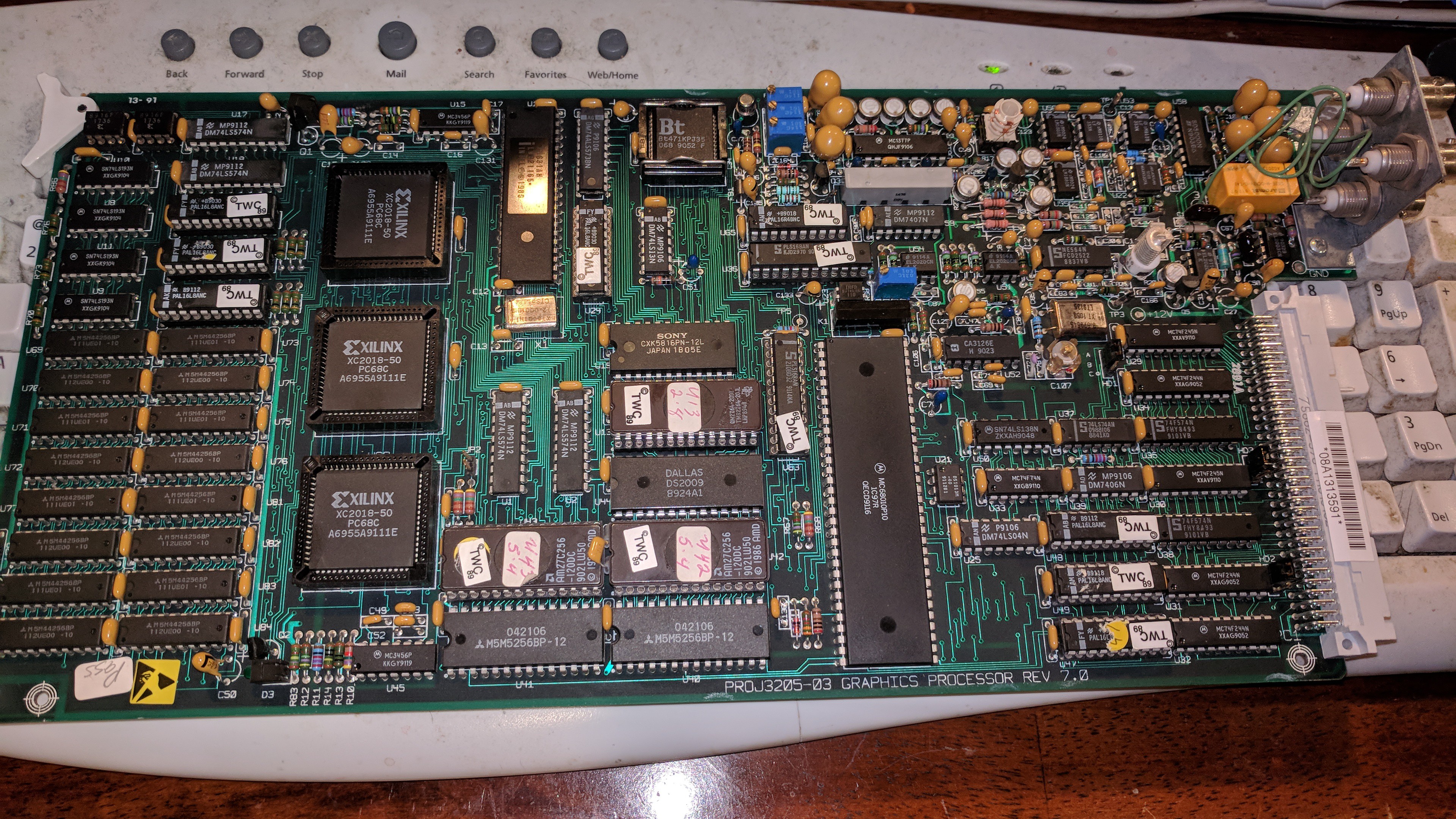
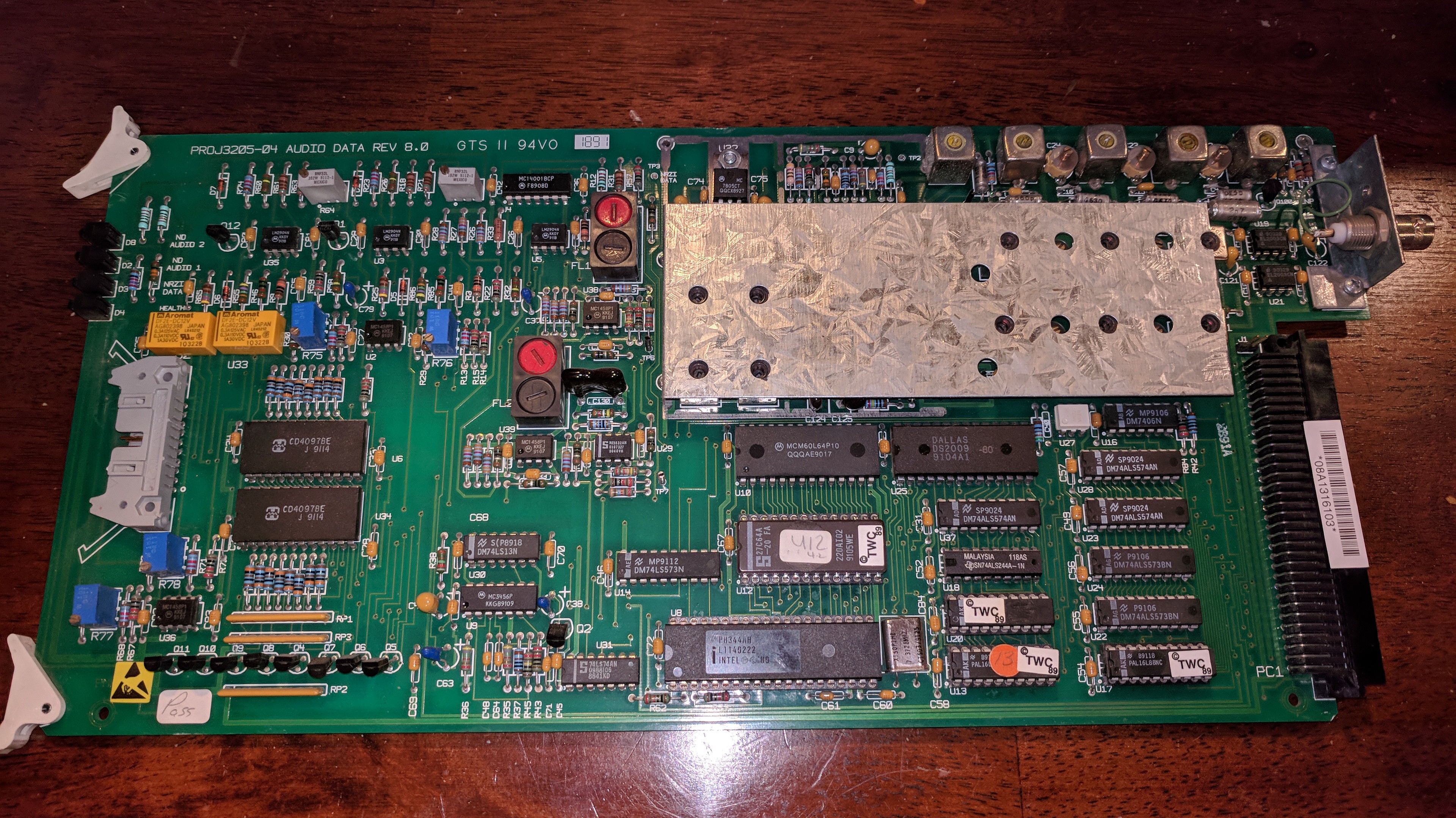
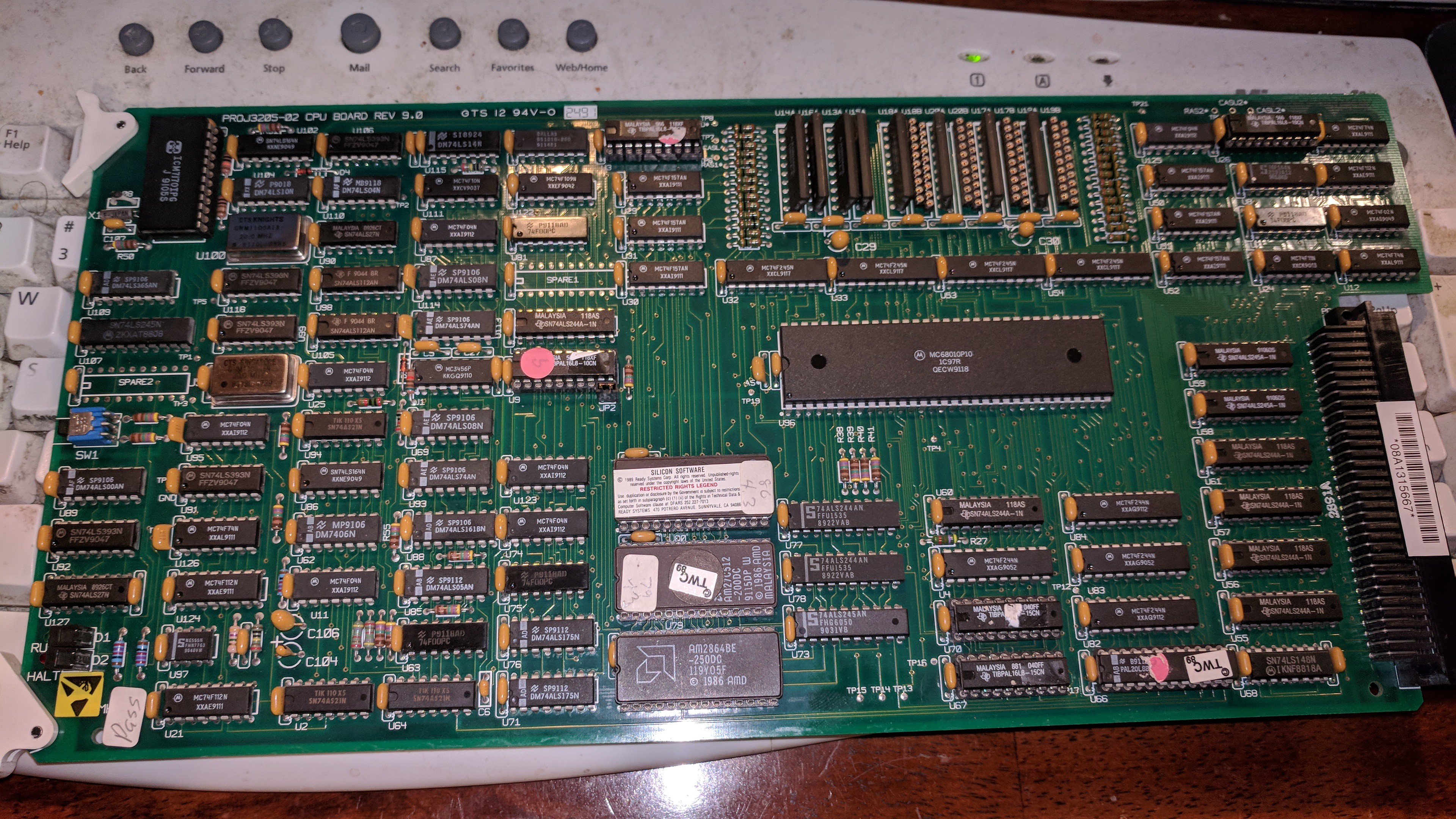
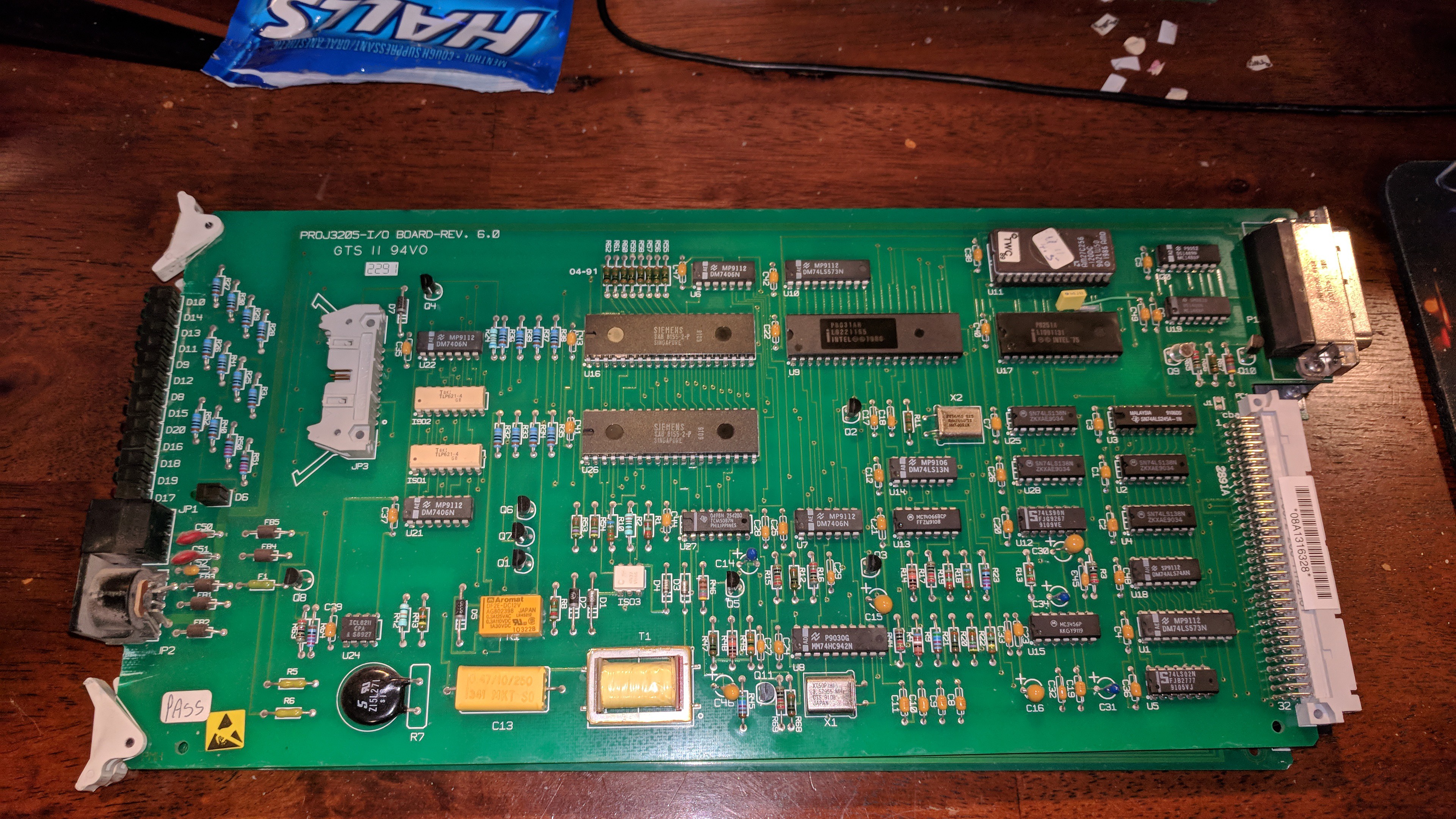
So the first thing I decided to do was stare at the PCBs a little bit to at least determine the hardware. And this is what I have gathered:
CPU Card: contains 4MB of DRAM, and an MC68010 CPU.
Graphics: This one is interesting. it contains an MC68010 CPU as well, AND an 8031 CPU (MCS51).
I/O card: Contains two PIO ICs and an 8031 CPU as well as a standard UART IC.
Data Card: This one is dual purpose, it has the audio and data circuitry on it as well as a 3-channel analog radio/RF stage for the various subcarriers. It contains an 8044 CPU which is a strange one. From what I could google, that chip is basically an 8051 with an SDLC controller instead of a serial UART. thats how I figured out what data it accepted, I was able to disassemble ROM to figure out how it initialized the SDLC transceiver.
Do I think this thing was overengineered? Probably. Maybe for futureproofing. But... there were alot of questionable design decisions, and what I think are blunders/bottlenecks. As we will see
Here is a video I published on youtube outlining the hardware:
Discussions
Become a Hackaday.io Member
Create an account to leave a comment. Already have an account? Log In.