 techknight
Up to this point, we have only focused on the basic architecture of the system and went into detail on the graphics card, and CPU card, only briefly mentioning the data and I/O cards.
But before we can begin to get a hello world program on the system, we must take a closer look at the I/O card.
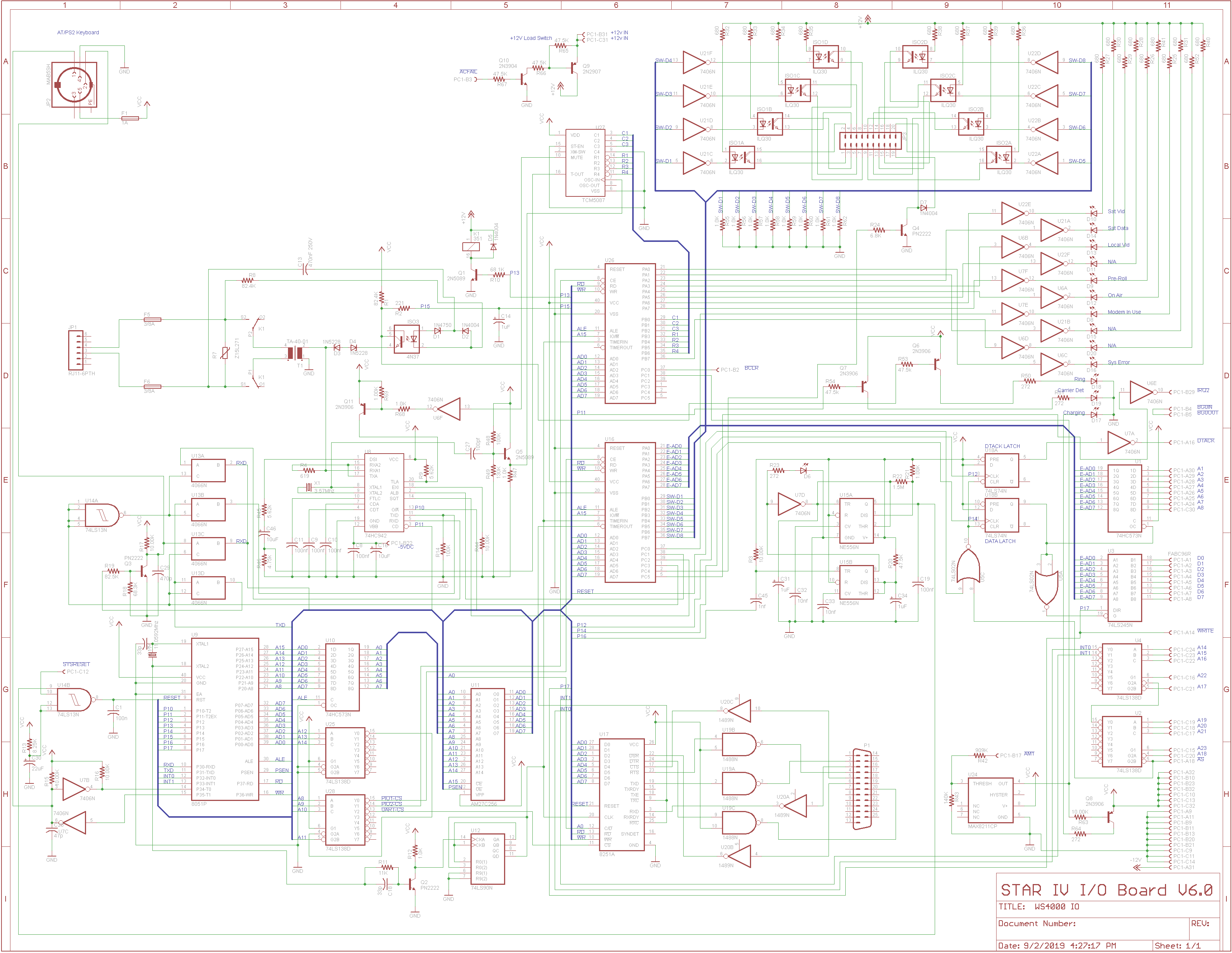
In a previous blog post, we mentioned the schematic of the I/O card, however to keep things simple, we will post the schematic again here:
With that, here is the system architecture of said card:
Peripheral - I/O Card

8051 Memory Map:
$0000 - $01FF = RAM
$0200 	      = UART Data
$0201         = UART Command
$8000         = PIO1 Command/Status Register
$8001         = PIO1 PORTA (VME Address/Data AD1-AD8)
$8002         = PIO1 PORTB (Rear External Switches 1-8)
$8003         = PIO1 PORTC (Various)
$8004         = PIO1 TCNT0 Low
$8005         = PIO1 TCNT0 High
$8100         = PIO2 Command/Status Register
$8101         = PIO2 PORTA (Indicator LEDs)
$8102         = PIO2 PORTB (DTMF Dialer Codes, 1 Indicator LED)
$8103         = PIO2 PORTC (Bus Clear, Charging Indicator)
$8104         = PIO2 TCNT0 Low
$8105         = PIO2 TCNT0 High

I/O Card VME Addressing:
$C00000 to $C001FF = 8051 INT0
$C04000 to $C041FF = 8051 INT1

PIO-1:
PA0: VME Address/Data 0
PA1: VME Address/Data 1
PA2: VME Address/Data 2
PA3: VME Address/Data 3
PA4: VME Address/Data 4
PA5: VME Address/Data 5
PA6: VME Address/Data 6
PA7: VME Address/Data 7

PB0: Switch 1
PB1: Switch 2
PB2: Switch 3
PB3: Switch 4
PB4: Switch 5
PB5: Switch 6
PB6: Switch 7
PB7: Switch 8

PC0: (LED 7) Modem In Use LED
PC1: Modem ALB
PC2: Modem SQT
PC3: Modem/AT Serial Select
PC4: Cube Relay Control
PC5: VME IRQ2

PIO-2:
PA0: (LED 10) System Error LED
PA1: (LED 8) Spare LED
PA2: (LED 2) Sat Data LED
PA3: (LED 3) Local Video LED
PA4: (LED 6) On Air LED
PA5: (LED 4) Spare LED
PA6: (LED 1) Satellite Video LED
PA7: (LED 5) Pre-Roll LED

PB0: DTMF Keypad Column 1
PB1: DTMF Keypad Column 2
PB2: DTMF Keypad Column 3
PB3: DTMF Keypad Row 1
PB4: DTMF Keypad Row 2
PB5: DTMF Keypad Row 3
PB6: DTMF Keypad Row 4
PB7: (LED 9) Spare LED

PC0: VME IACK2
PC1: Battery Charging Indicator
PC2 - PC5 unused.
This is basically where everything is hooked up as far as the address map. Essentially, it is an 8051 based card, with two PIO/RAM ICs, and a UART IC.
The card handles the LEDs, a modem, AT keyboard, serial port, and some general purpose I/O.
The funny thing about this card however, is the 68K bus interface logic and timing. It is all software-based and its controlled via interrupt on the 8051, so the interrupt execution time has to be in-step with the 68K Bus Cycles. absolutely insane, and there is NO room for timing variances or error on the bus read/write interrupt handlers or errors will ensue. I tried it.
One thing i noticed right away on the design of this particular card, is how there is an inverter off of the Q output on the flipflop, instead of just using the /Q output. As seen here:
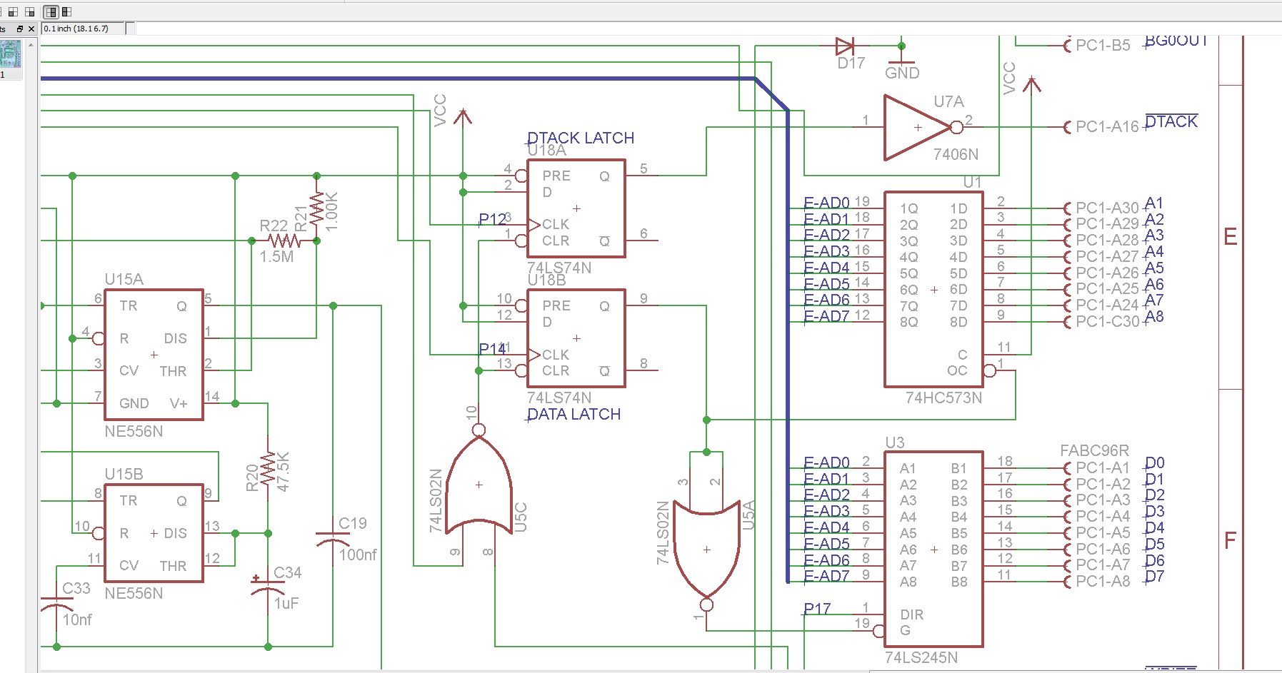
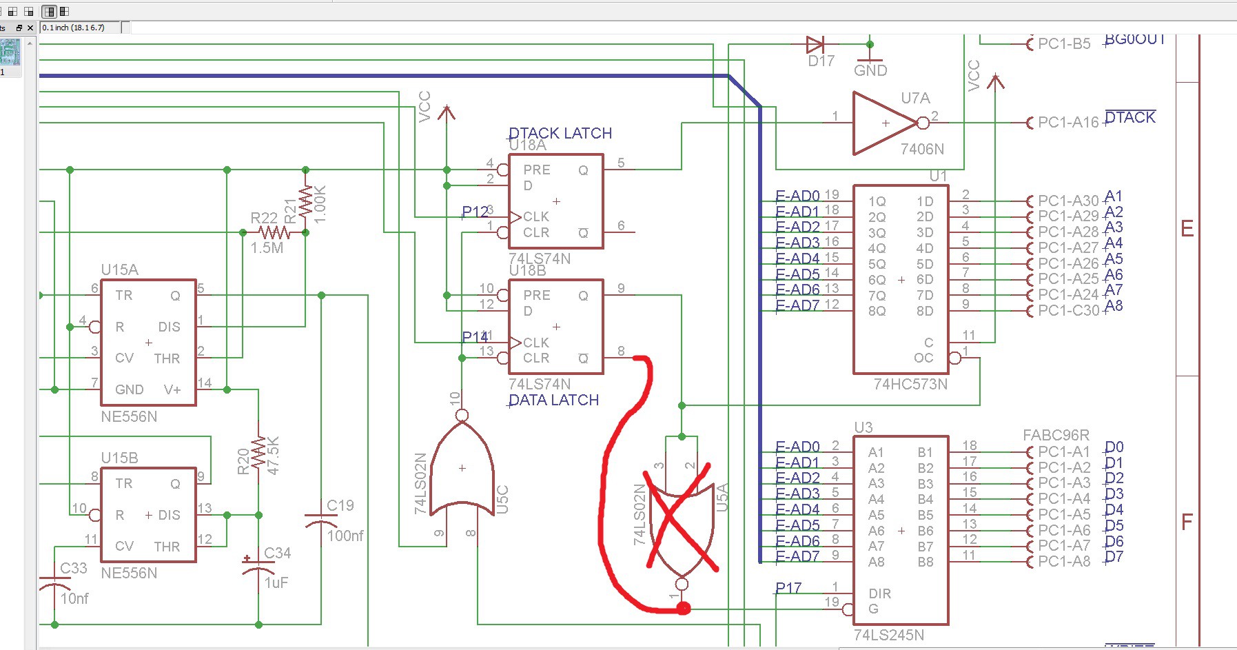
This part made no sense to me. You would save a gate if you just wired the /Q output instead of using a makeshift inverter. Maybe there is a timing reason? Honestly, I do not know.
In the next part, we need to disassemble the ROM and take a look at what is going on, since we have no driver or any details on how to drive this card.
Discussions
Become a Hackaday.io Member
Create an account to leave a comment. Already have an account? Log In.