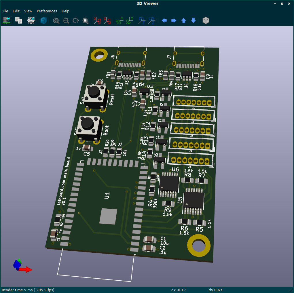
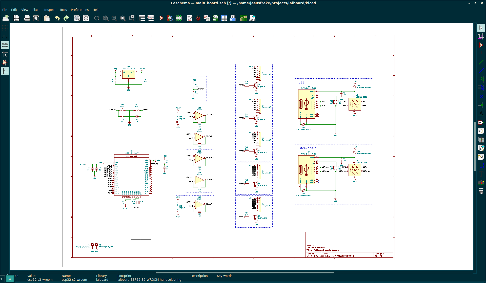
I've been spending some time designing and prototyping the new main board. There are a number of improvements compared with the v1 board (in addition to just being an actual PCB, rather than the ad-hoc thing using the vinyl cut process).


At first, I was thinking I would use an esp32s2 dev board, like the saola board, and just have a header socket for it on the main board. But I eventually came to the decision that it would be better to go a bit "lower level" and design a board around the raw esp32s2-wroom module.
For one thing, the saola dev board is fairly large, and would be hard to fit along with everything else needed in the space under the handrest. But it also uses a serial<->usb converter chip, instead of exposing the actual usb interface. You can still wire up a separate usb port to the gpio 18 and 19 pins, but that's a lot of wasted board space on an unneeded usb connector and serial conversion chip.
A few of the features/improvements:
- USB C port (because USB C >>> USB micro)
- It has a second USB C port for communication between the two halves. Although this isn't a real USB port. The actual communication will be a serial link over the D+ and D- pins. I didn't particularly like using a USB port for non-USB communication, but the best alternative I could come up with was a TRRS jack -- which isn't really hot-pluggable (e.g. shorting pins when you insert/remove a plug). So supporting hot-plugging won out over my concerns about confusion over the 2 different usb-c ports on each half.
- It uses discrete transistors to select each individual cluster (row) when scanning the matrix. Previously, it used an LED driver chip, but it was a bit of an expensive, specialty chip. Using discrete NPN transistors is cheaper, and they're much more ubiquitous.
One of the more significant changes is that it now uses transimpedance amplifiers to read the signals from the phototransitors, which you can read more about in my previous post.
I honestly didn't want to go that route initially, because it adds yet more components and complexity, and required embiggening the board. But I just wasn't happy with the phototransistor response times.
I do think it was the correct decision though, and it should help ensure more reliable operation of the optical switches, and enable even lower power usage due to lower LED currents and shorter duty cycles. Power usage isn't necessarily a huge concern atm, with a usb-powered device... But since it's using a bluetooth-capable chip, I won't rule out a battery powered bluetooth device in the future :)
 Ben Gruver
Discussions
Become a Hackaday.io Member
Create an account to leave a comment. Already have an account? Log In.