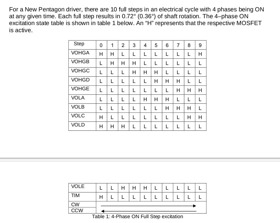
This is a simple full step sequence. It does not implement half stepping or any microstepping options. The CPLD is large enough to put a half step seqencer into it, but I don't think a microstepping sequencer would fit. The step signal is used as a clock signal for the sequencer. The RSTN reset signal and DIR direction input signal control the operation of the sequencer.
Another snippet from Oriental Motor's documentation shows the phase sequence required to drive these motors.

In full step mode, there are 10 unique states that repeat infinitely based on the Step and Direction inputs to the Step Sequence Generator. This sequencer is implemented in Verilog and synthesized using Xilinx's proprietary tool chain called ISE.
`timescale 100ns/100ns

// revised 1/21/2021 from table in 5PhaseNewPentBipolarDriver.pdf

module StepDriver_FullStep (
  input wire    rstn,       // system reset signal
  input wire    step,       // step input really a clock signal
  input wire    dir,        // direction input
  output wire   pha_hi,     // Phase A high side output
  output wire   pha_lo,     // Phase A low side output
  output wire   phb_hi,     // Phase B high side output
  output wire   phb_lo,     // Phase B low side output
  output wire   phc_hi,     // Phase C high side output
  output wire   phc_lo,     // Phase C low side output
  output wire   phd_hi,     // Phase D high side output
  output wire   phd_lo,     // Phase D low side output
  output wire   phe_hi,     // Phase E high side output
  output wire   phe_lo      // Phase E low side output
);
  reg  [9:0] seq;           // Sequencer registers
  wire [9:0] seq_next;      // Next state for sequencer registers

  // generate the next state data for the sequencer based on the current
  // sequencer value and the dir line.
  assign seq_next = dir ?  {seq[8:0],seq[9]} : {seq[0],seq[9:1]};

  // Instantiate the state register
  always @(negedge rstn or posedge step)
  if (rstn==1'b0)
    seq <= 10'b0000000001;
  else
    seq <= seq_next;

  // generate the phase signals from the one hot sequencer
  assign pha_hi = seq[0] | seq[1] | seq[9]; //|{seq[3:0]};
  assign phb_hi = seq[1] | seq[2] | seq[3]; //|{seq[4:1]};
  assign phc_hi = seq[3] | seq[4] | seq[5]; //|{seq[5:2]};
  assign phd_hi = seq[5] | seq[6] | seq[7]; //|{seq[6:3]};
  assign phe_hi = seq[7] | seq[8] | seq[9]; //|{seq[7:4]};

  assign pha_lo = seq[4] | seq[5] | seq[6]; //|{seq[8:5]};
  assign phb_lo = seq[6] | seq[7] | seq[8]; //|{seq[9:6]};
  assign phc_lo = seq[0] | seq[8] | seq[9]; //|{seq[9:7],seq[0]};
  assign phd_lo = seq[0] | seq[1] | seq[2]; //|{seq[9:8],seq[1:0]};
  assign phe_lo = seq[2] | seq[3] | seq[4]; //|{seq[9],seq[2:0]};

endmodule
The timescale line at the top of the file is used for simulation. I used Icarus Verilog and GTKWave for simulating the file. The testbench file that drives the simulation is not shown here. The timescale statement does not effect the synthesis results at all.
The "module" statement assigns a name to the module.
Following the module statement is the port list. All of the input and output signals of the module are defined, along with their direction and types.
Next, the counter registers and next state generation logic signals are defined. In school, we were taught to design state machines with counter logic and decoding the counter values to drive the output signals. This state machine uses what is called a "One Hot" method rather than a counter to keep track of the state. It is implemented as a bi-directional 10 bit shift register. It is simpler to implement and simpler to decode than an actual binary counter would be.
Combinational logic generates the next state based on the value of the direction input signal:
// generate the next state data for the sequencer based on the current
// sequencer value and the dir line.
assign seq_next = dir ? {seq[8:0],seq[9]} : {seq[0],seq[9:1]};
This line controls the direction of the shifting by selecting the current state signals to the left or to the right of each bit for the next state. Note the "wrap around" at the end of the choices.
The 10 bit register holding the current state is reset to an initial value if the rstn signal is low, or the next state values loaded into the register on the rising edge of the step signal:
// Instantiate the state register
always @(negedge rstn or posedge step)
if (rstn==1'b0)
seq <= 10'b0000000001;
else
seq <= seq_next;
The reset value for the state sequence is 0000000001. That 1 value gets shifted left or right on each rising edge of the step signal. The reset signal is dominant over the step signal, so if the reset signal is asserted (low) it forces the state value regardless of the step signal. The reset signal is only driven low for 200mS at the power up of the board in this system.
Finally, the code that translates the current state into the phase control signals is at the bottom of the file. This code is what maps the current state into the Phase Sequence Table.
Implementing the half step sequence uses 20 states, and could be programmed into the CPLD instead of the full step sequence.
 Bharbour
Discussions
Become a Hackaday.io Member
Create an account to leave a comment. Already have an account? Log In.