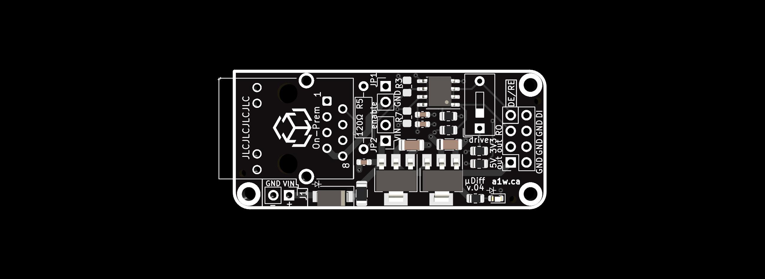
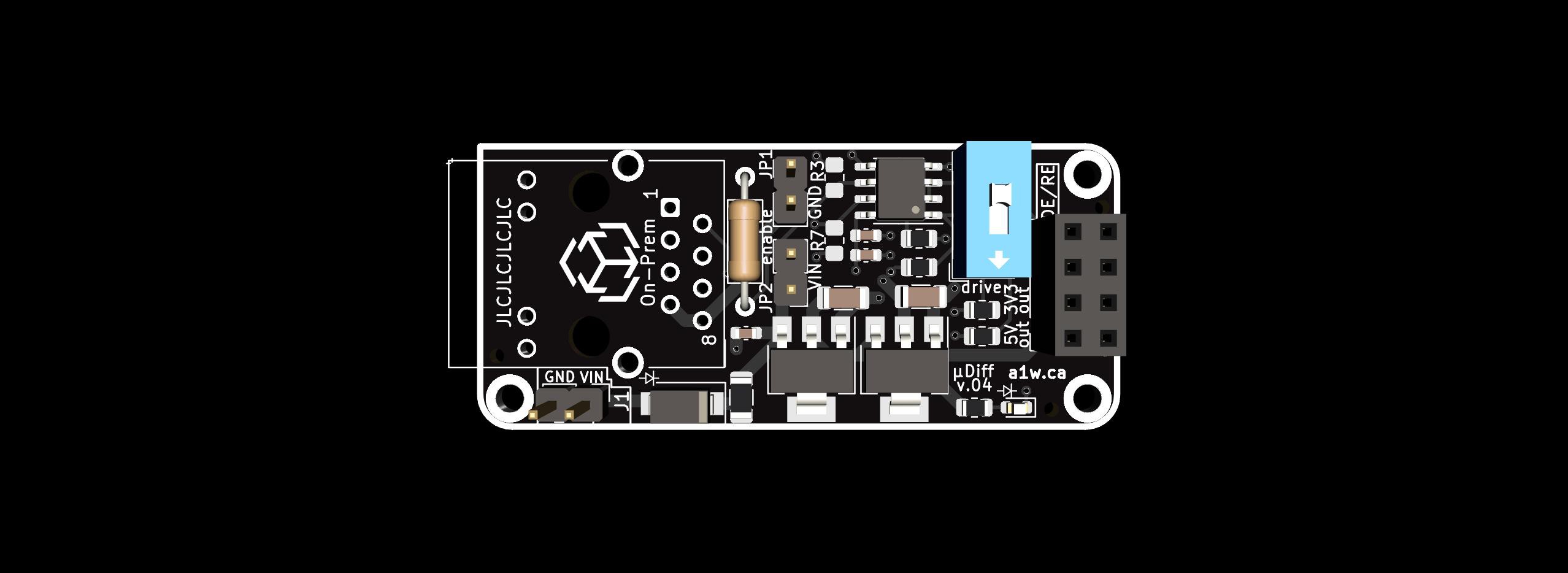
Here's a sneak preview of v.04:


It has some important changes which I'll list below:
- The PCB is now exactly HALF the width of the v.03, at 50x22mm (instead of 50x44mm).
- It's a 4-layer stackup instead of 2-layers, with 3.3V power and ground planes in the middle.
- Through-hole 5V DC-DC converter is now SMD but has a max 12V/1A (15V absolute max)
- Through-hole RS485 IC is now SMD and runs at 3.3V instead of 5V.
- Through-hole fuse is now SMD 24V/1A (trip 1.8A).
- GND and VIN are now simple pin headers instead of a large terminal block, since current is limited to 1A anyways.
- DE and RE pins are tied together (to GND with 10K resistor, i.e: receive mode), but can be set to drive mode (to 3.3V) through a DIP switch. This means it's not possible to disable the RS485 IC anymore.
- 8-pin JST output header is now a 2x4-pin female socket header, and since DE/RE are tied, there is now a third GND pin on the header.
- Jumpers JP1 and JP2 can enable sending GND and VIN through the RJ45 connector. Previously only VIN had a jumper and GND was always connected through the cable.
- Resistors R3 and R7 are unpopulated 0805 pads for 20K biasing resistors on the A/B differential pair (A to 3.3V, B to GND).
- There is a 10K pullup resistor on the RO line, and a 10K pulldown resistor on the DI line.
- RJ45 shield pins are now grounded.
- Capacitors are all ceramic instead of electrolytic.
- Mounting holes are now M2 instead of M3 and they are NOT grounded anymore.
- There is a new blue Power LED indicator at the edge of the board.
- Changed the shape of the PCB and removed one mounting hole. The asymmetry would make it impossible to mount incorrectly in an enclosure (a legit problem I had with v.03).
That's a lot of changes, but why?
It's been over a year since I designed the v.03 board, and I've learned quite a bit more about RS485. In particular, I realized that "forcing" biasing resistors on every device, was not a good idea. Typically one might only need biasing resistors on ONE device on the bus.. not all of them. Also since the device is not always connected to an MCU, I made sure the default configuration forces the device into Receive mode by pulling down the RE line with a 10K resistor, rather than pulling it up like in v.03.
It's also not always required to send GND through the RJ45 cable (as a common ground) depending on the environment.
Since those things are user-defined, I picked the sane default to pull-down DE/RE, and leave the other pads unpopulated for those who "know what they want" - and 0805s should be reasonably easy to add by those who "know what they're doing".
Finally, I wanted a much smaller and more compact board with less through-hole components.
What functionality changed?
Pretty much nothing changed from a functionality perspective, except for the lower VIN (was previously max 28V).
Is this available yet?
No, I just sent them to be manufactured, so I expect to have and test these boards around the middle or end of August (latest).
 Alexander Williams
Discussions
Become a Hackaday.io Member
Create an account to leave a comment. Already have an account? Log In.