UPDATE: September 06, 2022
In a previous post I said I won't make many changes to v.04, but it turns out there were more than a few things I didn't like about it.
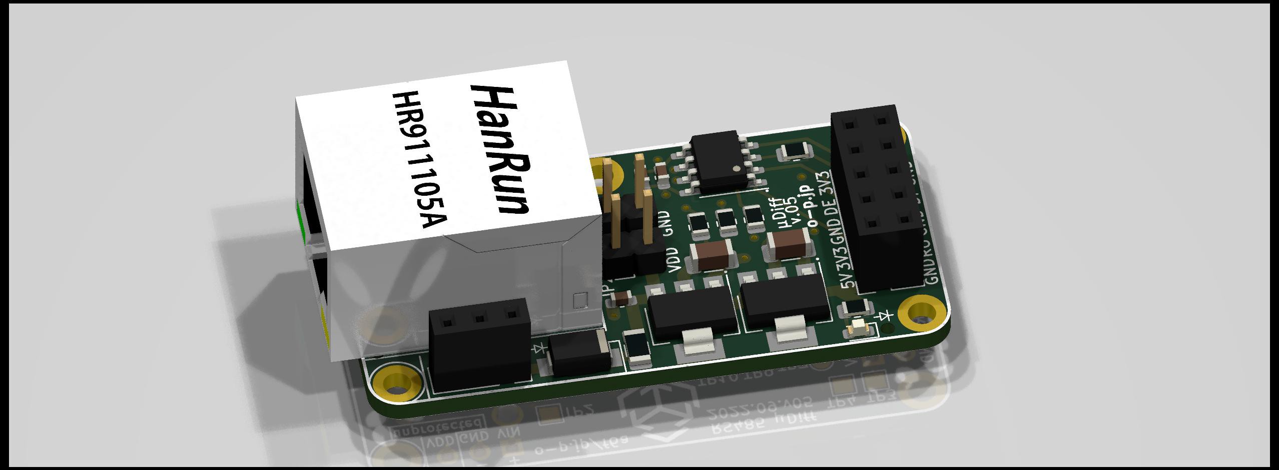
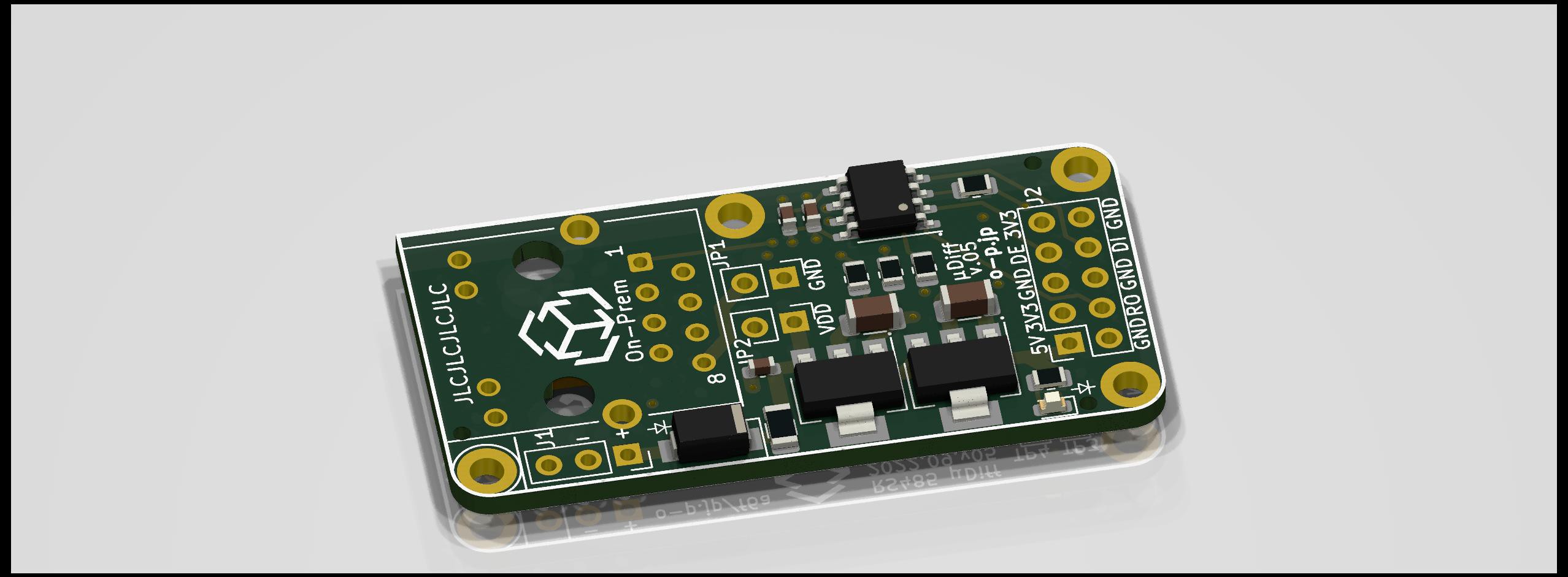
In v.05, I've made the following improvements:

- Changed dimensions slightly, to 46mm x 22.5mm to accommodate the changes below.
- Re-added a 4th mounting hole, because the PCB won't stand on 3 legs haha.
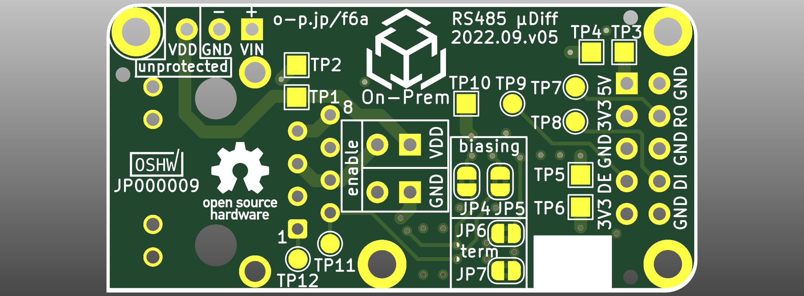
- Replaced the through-hole "optional" terminating resistor (120Ω) with an 0805 SMD 100Ω resistor to match the characteristic impedance of a CAT5e or CAT6 cable. In a multi-drop configuration, the resistor can be enabled by soldering two bridge jumpers on the bottom of the board: JP6 and JP7.
- Added 2 x 0805 SMD 390Ω fail-safe biasing resistors which can be enabled by soldering two bridge jumpers on the bottom of the board: JP4 and JP5.
- Added a 3rd input pin for VDD on the header J1, which will bypass the diode and fuse and go directly to the 5V DC-DC converter and the RJ45 connector (if the VDD jumper JP2 is enabled).
- Changed the orientation of the VDD/GND 2-pin jumpers JP1 and JP2.
- Added test pads under the PCB for every signal and power rail.
- Updated silkscreens on the top and bottom of the PCB.
- Replaced 2x4 pin (8P) socket header with 2x5 pin (10P) and added an extra 3.3V and GND pair.
- Removed the 10K pullup resistor on DE/RE.
- Removed the DIP switch to enable "drive" mode. Simply tie DE to 3V3 with a jumper wire to enable "drive". Defaults to "receive" mode.

Here's a preview of the bottom of the PCB, and the new testpads and solder bridge jumpers for enable biasing/terminating:

As a side note, for those who don't follow my GitHub account, I've already published the schematic and PCB files for v.04, but I haven't updated the documentation since I don't plan on selling v.04. The updated documentation (for v.05) will be published once I confirm it's working as expected.
Stay tuned!
 Alexander Williams
Discussions
Become a Hackaday.io Member
Create an account to leave a comment. Already have an account? Log In.