Onboard Programmers are great
On microcontroller development boards (such as ST Nucleo Boards) it's very handy to have an integrated JTAG programmer/debugger. If you would like to build your own board with an embedded programmer, things get a bit tricky.
In the case of the STMicroelectronics® popular ST-Link V2.0/V2.1 there are lots of clones out there, e.g. from eBay/AliExpress.
The maximum programming speed of those is 4 MHz. For larger projects, this can cause long upload times of up to a minute, which is not very pleasant while debugging a system.
The "new" ST-Link V3 does not have this issue and provides a Full-Speed USB interface, which leads to an upload speed of 24 MHz!
No ST-Link V3 clones available
In my latest project, I would like to implement an embedded ST-Link V3, but I couldn't find any resources of other people who have done that already.
Therefor, I've started reverse engineering things and created a proof of concept in the form of an external ST-Link V3 prototype.
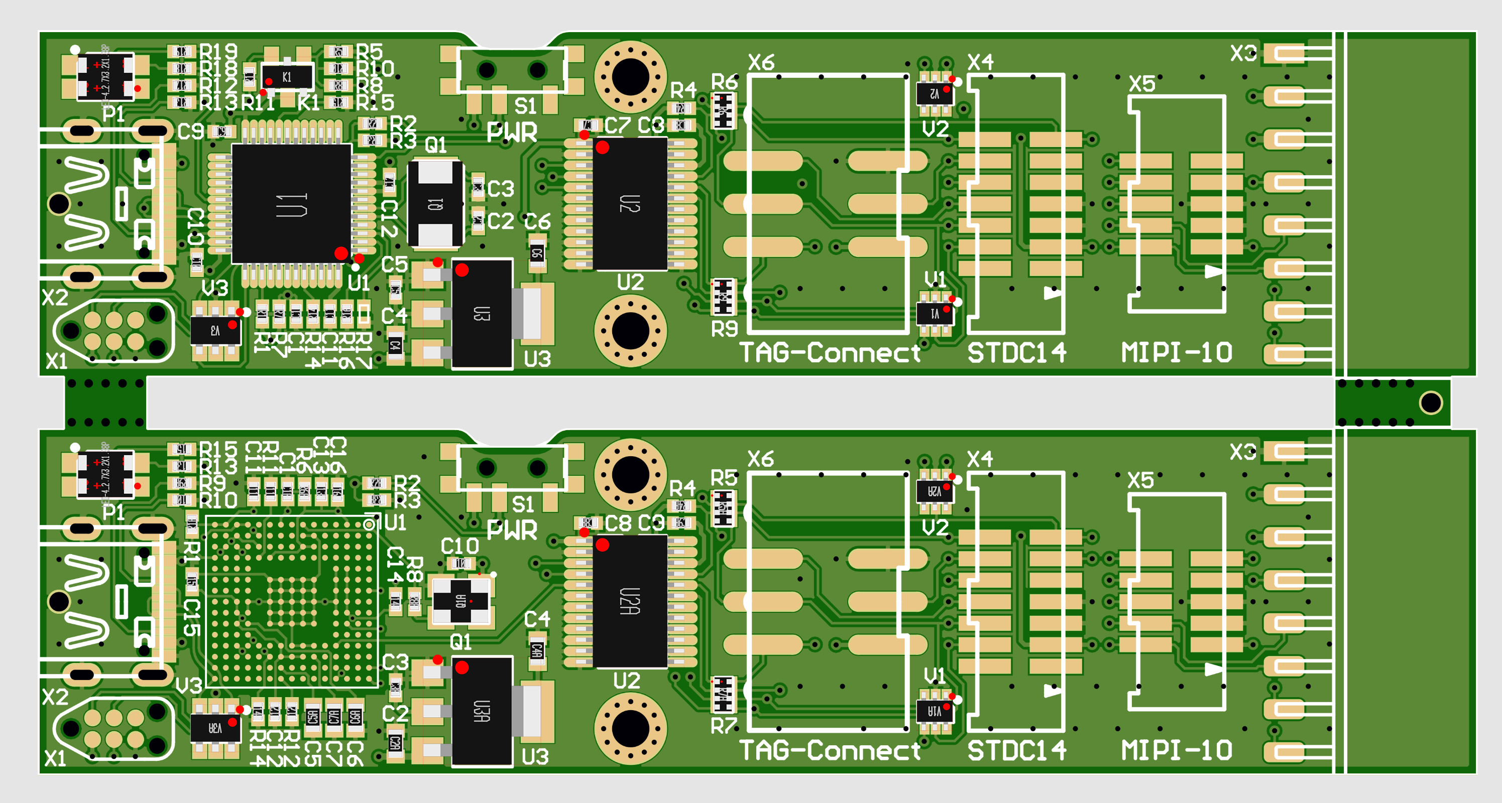
Instead of developing only a cloned ST-Link V3, I decided to build a custom ST-Link V2 programmer in addition.
My goal was, that they share the same physical dimensions and are easily exchangeable.
Hardware Design
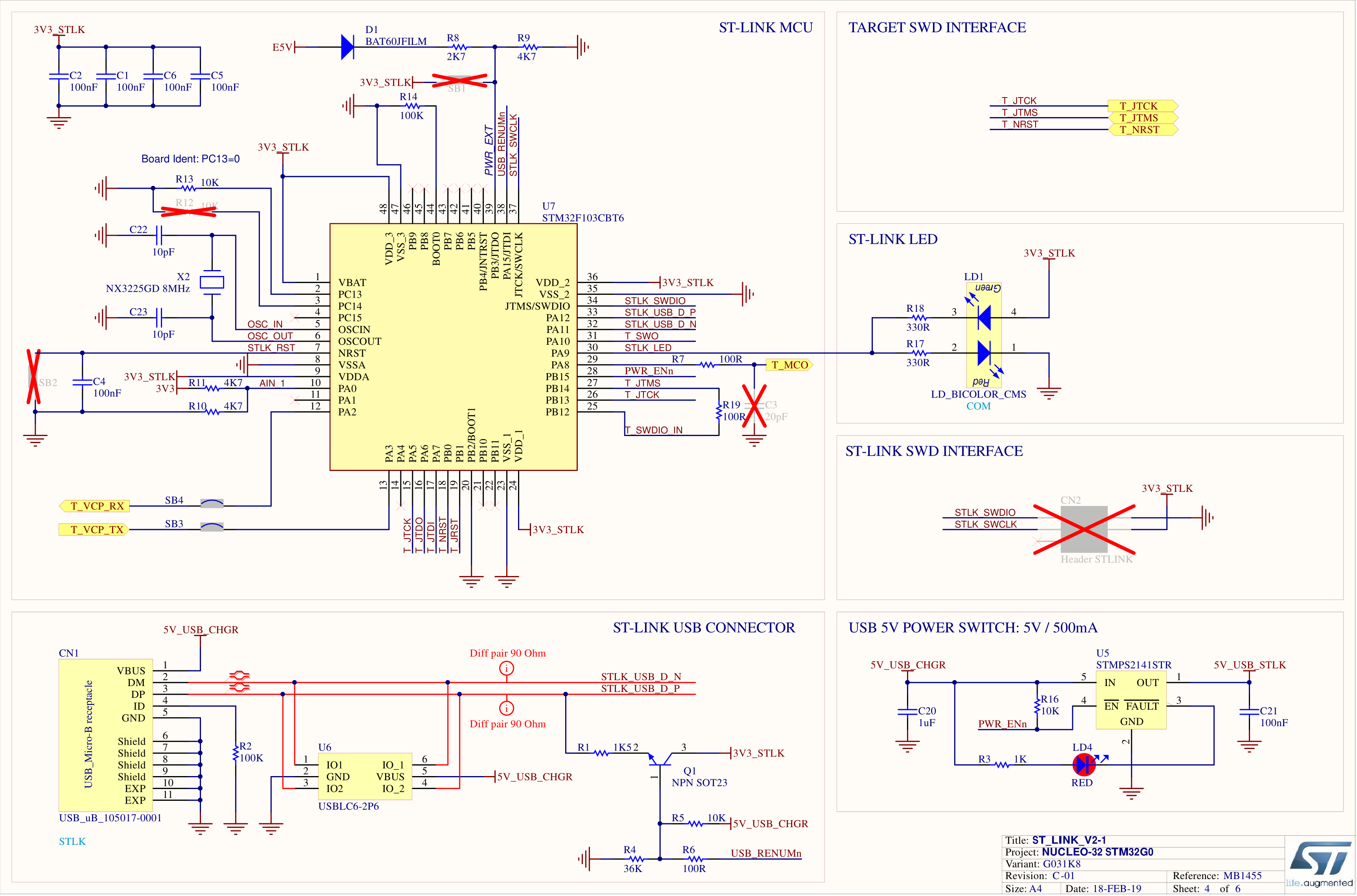
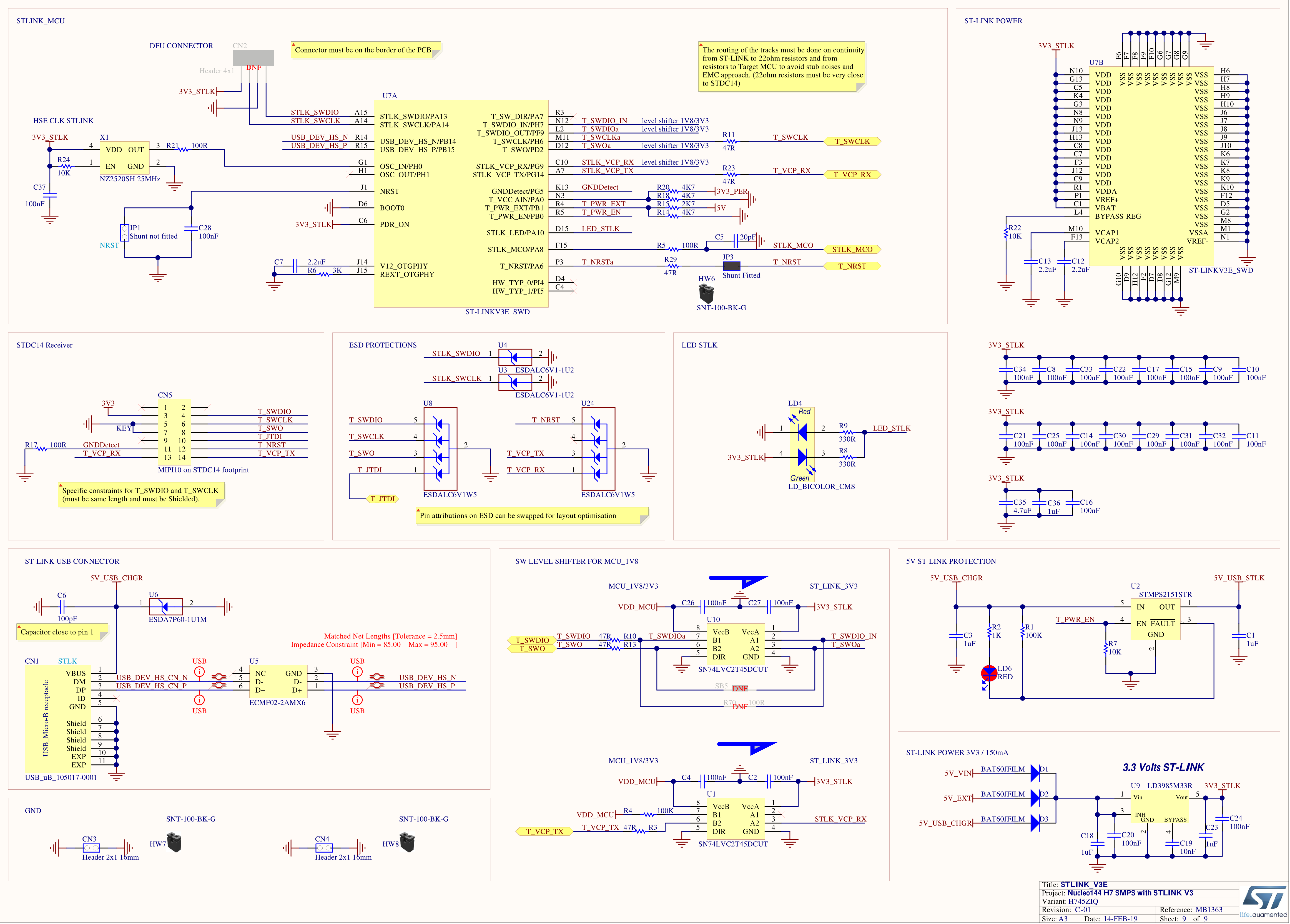
As reference for designing my own hardware, I used schematics of ST Nucleo boards:
ST-Link V2.1: NUCLEO-32 STM32G0 (MB1455)

ST-Link V3.0: NUCLEO-144 STM32H7 (MB1363)

Some pins of the onboard programmer are sadly not shown in this schematic. Luckily, some other guys on the EEV-Blog did already some reverse engineering of the pinout of the ST-Link V3 (EEV-Blog). Here is what they've come up with:
CN3-1            VDD
CN3-2            PA14 (SWCLK)
CN3-3            GND
CN3-4            PA13 (SWDIO)
CN4-1            GND
CN4-2            nRST
CN5-2            PB14            (USB DM)
CN5-3            PB15            (USB DP)
1                PB11            Bridge UART RX(1)       -> RX signals are inputs for STLINK-V3MODS, outputs for target.
2                PD11            Bridge UART CTS
3                PD12            Bridge UART RTS
4                PH7             T_JTMS/T_SWDIO
5                PG5             GNDDetect(2)
6                PC7             T_JTDO/T_SWO(3)
7                PA9             Bridge SPI CLK
8                GND             GND
9                PA11            Bridge CAN RX(1)
10               PA12            Bridge CAN TX(4)
11               PC10            Bridge UART TX(4)       -> TX signals are outputs for STLINK-V3MODS, inputs for target.
12               PG9             T_VCP_TX
13               PB3             T_JCLK/T_SWCLK          (SWO)
14               PB4             Bridge SPI NSS
15               PG14            T_VCP_RX
16               PB6             Bridge I2C SCL
17               PB9             Bridge I2C SDA
18               PE2             Bridge GPIO0
19               PE4             Bridge GPIO1
20               PE5             Bridge GPIO2
21               PE6             Bridge GPIO3
22               (LoadSW out)    Reserved(5)
23               PC1             Bridge SPI MISO
24               GND             GND
25               PC2             Bridge SPI MOSI
26               GND             GND
27               GND             GND
28               PA1,PF8         T_JTDI/NC(6)
29               GND             GND
30                               T_VCC(7)
31               PA6             T_NRST
32               PA7             T_SW_DIR
                 PA0             T_VCC (pin 30), divided down
Load_EN          PB0             (load_EN (w 10k pulldown)
OSC 25MHz        PH0 OSC-IN
(VBUS detect?)   PB1/ADC?        (Vsw divided by (4.7k+2.7k))
LD1_1            PA10            (through 330 ohm)
LD1_2            PA10            (through 330 ohm)
LD1_3            GND
LD1_4            VDD             3.3V
LD2                              ST-Link fault           Load-switch Fault
LD3              5V/VBUS?        5V power + resistor
Manufacturing
The PCBs have been manufactured and assembled by JLCPCB. All files are available to download below.
To save some production costs, I decided to combine both ST-Link versions on one PCB. They can be separated by breaking at the specified mouse bite holes.

The missing parts are hand placed and soldered with a heat gun.
Firmware
The firmware of the ST-Link consists of two parts: Bootloader and application code.
Bootloader
The bootloader makes it possible to upgrade the ST-Link firmware via USB and the STM32CubeProgrammer. The bootloader itself doesn't get updated or changed in this process. By running the bootloader code, the JTAG-SWD Readout-Protection gets activated, which means that the firmware can't be dumped later on.
A guy named lujji established to dump the bootloader by uploading a "fake" firmware which sends the whole Flash content via UART. He documented this process on his webpage here.
He reverse engineered the bootloader code and patched out the instructions which activate the Readout-Protection.
All different bootloader variants (protected and unprotected) can be downloaded below.
Application Firmware
The actual application firmware on ST-Link differs for each type (V2.0 / V2.1 / V3.0), active features (STM8 and/or STM32, VCP, MSD) and revision. The easiest way to get the firmware is to download the ST-Link firmware update tool by ST.
This tool is written in Java and contains all firmware images in binary format, but they are encrypted as AES-128.
By decompiling the Java application lujji found the "secret" keys to decrypt the firmware images. He even made a tool to decrypt the files easily, available on GitHub.
To run the st-decrypt application just run this commands in your terminal:
For Version V2.x
java -jar st_decrypt.jar --key "best performance" -i encrypted.bin -o decrypted.bin
For Version V3.x
java -jar st_decrypt.jar --key " .ST-Link.ver.3." -i encrypted.bin -o decrypted.bin
As you can see, the password for decrypting the data is either "best performance" for V2.x and " .ST-Link.ver.3." for V3.x.
To find those secret keys this article was extremely useful!
I've decrypted all kinds of different firmware images. They can be downloaded from below.
Good to know is that if you once loaded the firmware on a freshly built ST-Link, it acts as an original. You can upgrade the firmware with the ST-Link updater tool as normal.
 Florian Baumgartner