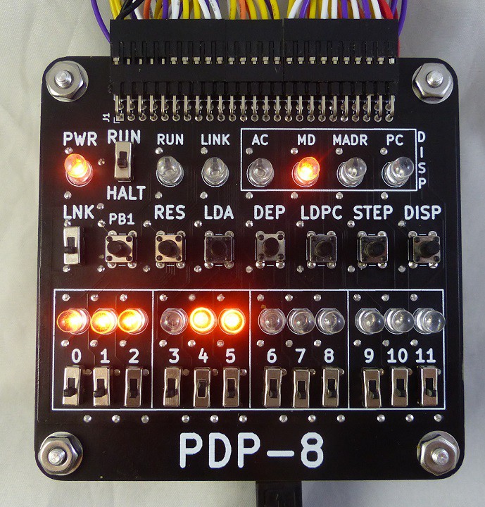
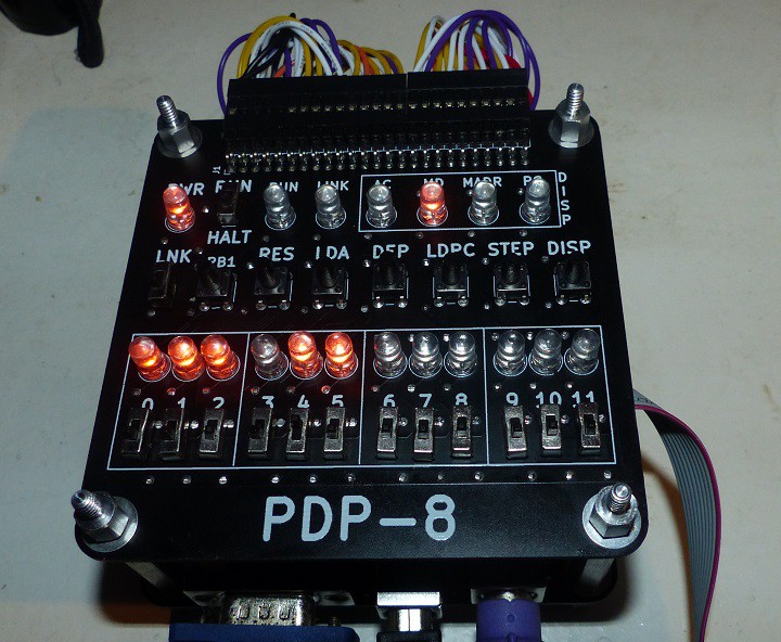
PCB arrived. Built it. Tested it. It took a lot of FPGA tweeks to get it working like I want.

Pushbuttons
- DISP - cycles between DISP LEDs [AC, MD, MADR, PC]
- STEP - single step the CPU
- LDPC - load the PC from the bottom slide switches
- DEP - store the value from the bottom slide switches to the memory at the current Program Counter
- LDA - load the Accumulator from the bottom slide switches
- RES - reset the CPU
- PB1 - spare
Slide Switches
- 0-11 value that is loaded by the pushbuttons. Also the address value in MD mode
- LNK - set the LINK bit when the accumulator is loaded (not yet implemented?)
- RUN/HALT - up = Run the CPU from the current PC, down = Halt the CPU
LEDs
- 0-11 - displays the value in the register/memory location selected by the DISP LEDs and selected by the DISP pushbutton
- PC - display the Program Counter value on 0-11 LEDs
- MADR - Not used
- MD - displays the data in memory at the current PC on 0-11 LEDs
- AC - displays the Accumulator value on 0-11 LEDs
- LINK - display the link bit (not yet implemented?)
- RUN - illuminated when the CPU is running, off when the CPU is halted
- PWR - power LED
Mounted above FPGA Card

 land-boards.com
Discussions
Become a Hackaday.io Member
Create an account to leave a comment. Already have an account? Log In.