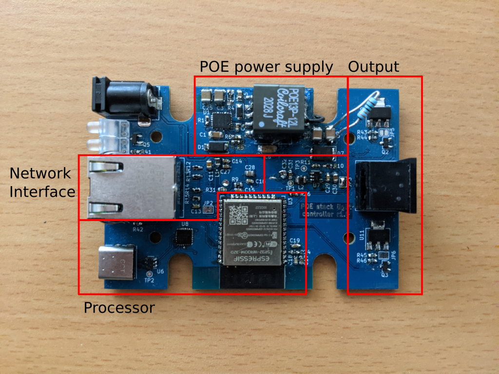
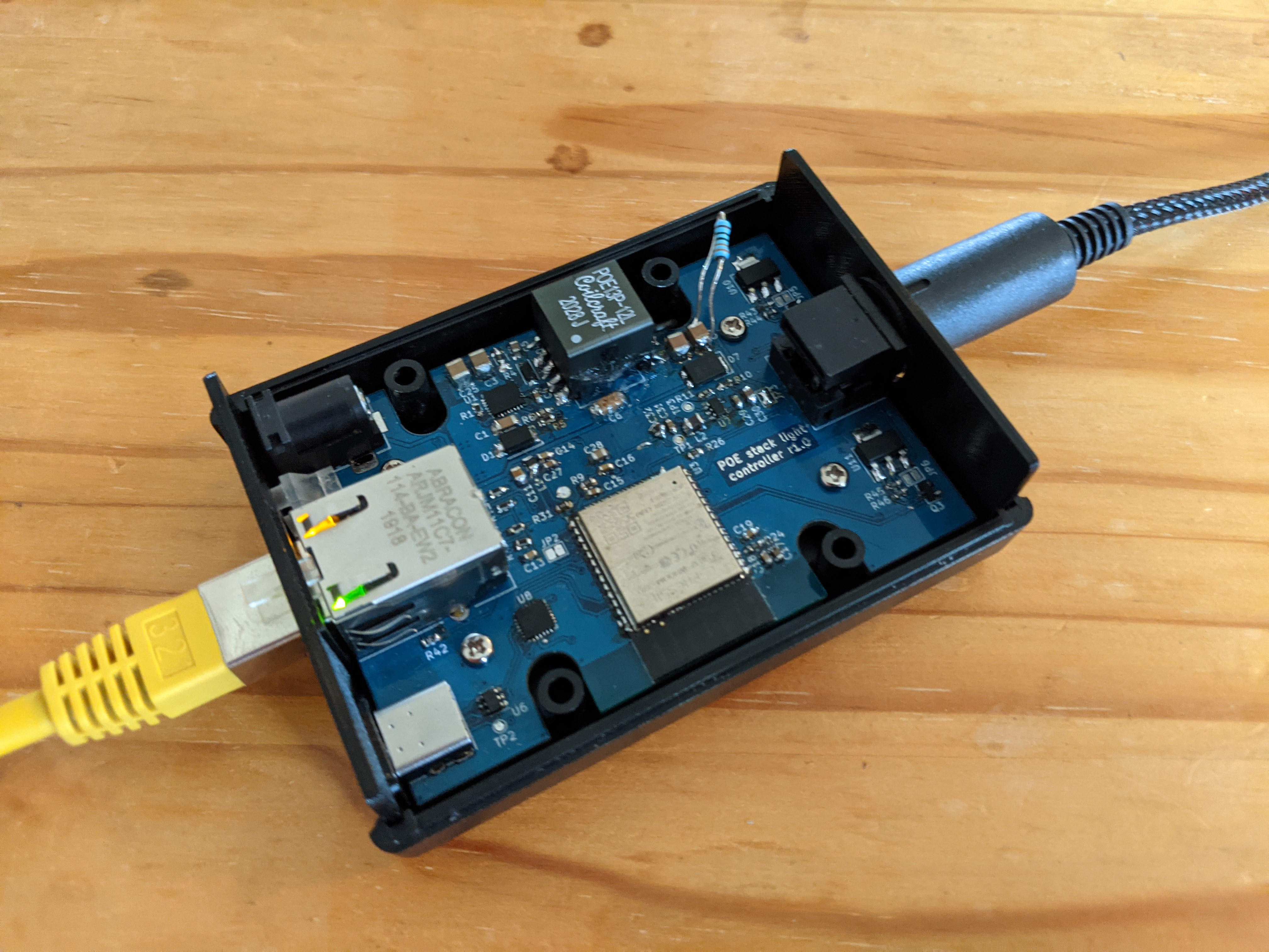
Following on from the second prototype a pcb design was created that merged the required components together. The only major addition from the prototype was the POE power supply hardware. The design is split into four major sections, the output stage, the POE power supply, the processor, and the network interface.

The stack light takes a common 12v input with switched grounds for each light segment and the buzzer. A mosfet switch was used to control each of the channels with brightness controlled by pwm from the microcontroller. As provided the light has a voltage regulator based current limiter shared across all the illumination channels, this prevents multiple segments from being lit at full brightness simultaneously. This was resolved by bypassing the current limit inside the light with a jumper wire and then adding a copy of the current limiter circuit in the light to the board for each of the three led channels, giving them their own current limit.
For the POE power input, a transformer setup rather than a switch mode design was used. The use of a transformer based design provides electrical isolation and allows other connections to be exposed without the risk of a short. The power over ethernet schematic is based off the MP8007 reference design. The catch with many of the reference designs for POE PD controllers is that the transformers used in them are not easily available, therefore, the transformer needed to be replaced with a more easily acquired Coil craft transformer requiring a change to many of the other components as well. A backup DC jack was also added in the event that something was wrong with the POE design.
An integrated ESP32 wireless module was used for the main processor. As the module isn't needed for its wifi capabilities the ESP32 could have been added as a standalone chip, however, using the module simplifies the design as compared to using the ESP32 IC directly and the extra board space occupied wasn't an issue. The large voltage drop from the main 12v supply required for the light to the 3.3v supply needed for the control circuitry prevents use of a linear regulator as this would produce quite a lot of heat. Instead a stepdown switch mode power supply was used to provide the 3.3v supply. A USB to serial converter was included to facilitate easy programming and give the option for a serial console interface if wanted.
The network interface uses the LAN8710A ethernet transceiver IC. This communicates to the ESP32 with the RMII protocol used for 100MB ethernet PHYs. In order to support the POE functionality an ethernet connector with internal magnetics that expose the centre taps of the cable side of the interface was chosen.
With the design sorted the PCB could be laid out. The PCB was designed to fit into an off the shelf enclosure in order to minimise the mechanical complexity of the project. The design has several SMT components with underside ground pads so large vias were added under each of these ICS to give access to these pads and enable hand soldering of the board. Other than that it was a fairly standard PCB creation process.

Once the boards arrived and the first unit assembled a couple of issues were discovered. The most problematic was that the POE transformer output was reversed which was fixed by soldering wires to the correct locations. In addition the ESP32 draws less power than the minimum to maintain powered over POE so an additional load resistor was added to draw the required power. The other notable problem is that the POE transformer has a high pitched wine when at low power which has yet to be solved. The board was otherwise functioning and worked with the firmware that has been used on the second prototype. The next stage is to complete the missing software features and then the project will be ready to use.
For those interested the hardware designs can be found on github.
 Tyler Ward (Scorpia)
Discussions
Become a Hackaday.io Member
Create an account to leave a comment. Already have an account? Log In.