 zaphod
In my last post I discussed some of the problems I had with the version 1 hardware at the end of 2019. There were enough issues with the hardware that I decided that it would be worth redoing the board and so I started a version 2 design, but didn't get very far before school started again and I had to put the project on hold.
In 2020 I started working on my undergraduate capstone project, and the combination of capstone work and regular school work/internship work meant that I didn't end up having enough time to work on this project for all of 2020.
After finishing school in April of 2021 I had some more free time again and dug out this project and reevaluated what I'd completed so far.
Rather than moving forward with the V2 hardware design, which wasn't well developed and had been rushed at the end of 2019 I decided to start fresh with a V3 hardware design that would address many of the issues I faced with the V1 hardware.
I ended up making the following changes and simplifications to the V1/2 designs:
- move voltage regulation off the board (3v3 power supplies are easy to come by and there's not much value in adding a regulator to the board)
- fix as much of the wiring as I could (e.g. the 3v3 line on the ICSP header)
- move the master oscillator off board. Since I wanted this to be flexible anyway there is no point in adding it to the main PCB
- better protection on the USB curcuit (added TVS diodes and grounded the USB shield)
- Rather than trying to get the micro to FPGA wiring correct I decided to just break everything out to a pin header and connect GPIOs manually
- this basically make the board a reusable devboard with an FPGA and micro on it, but it was supposed to save me from needing another revision of the hardware if I managed to mess up connections again
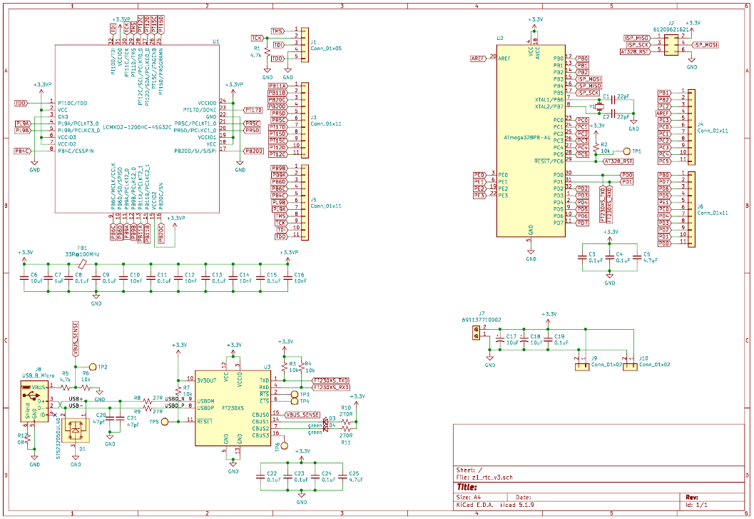
With these simplifications in mind I went ahead and redesigned the board with the same parts as the version 1 design from 2 years ago. The final schematic is as follows:
I ordered and assembled the boards which looked like this:
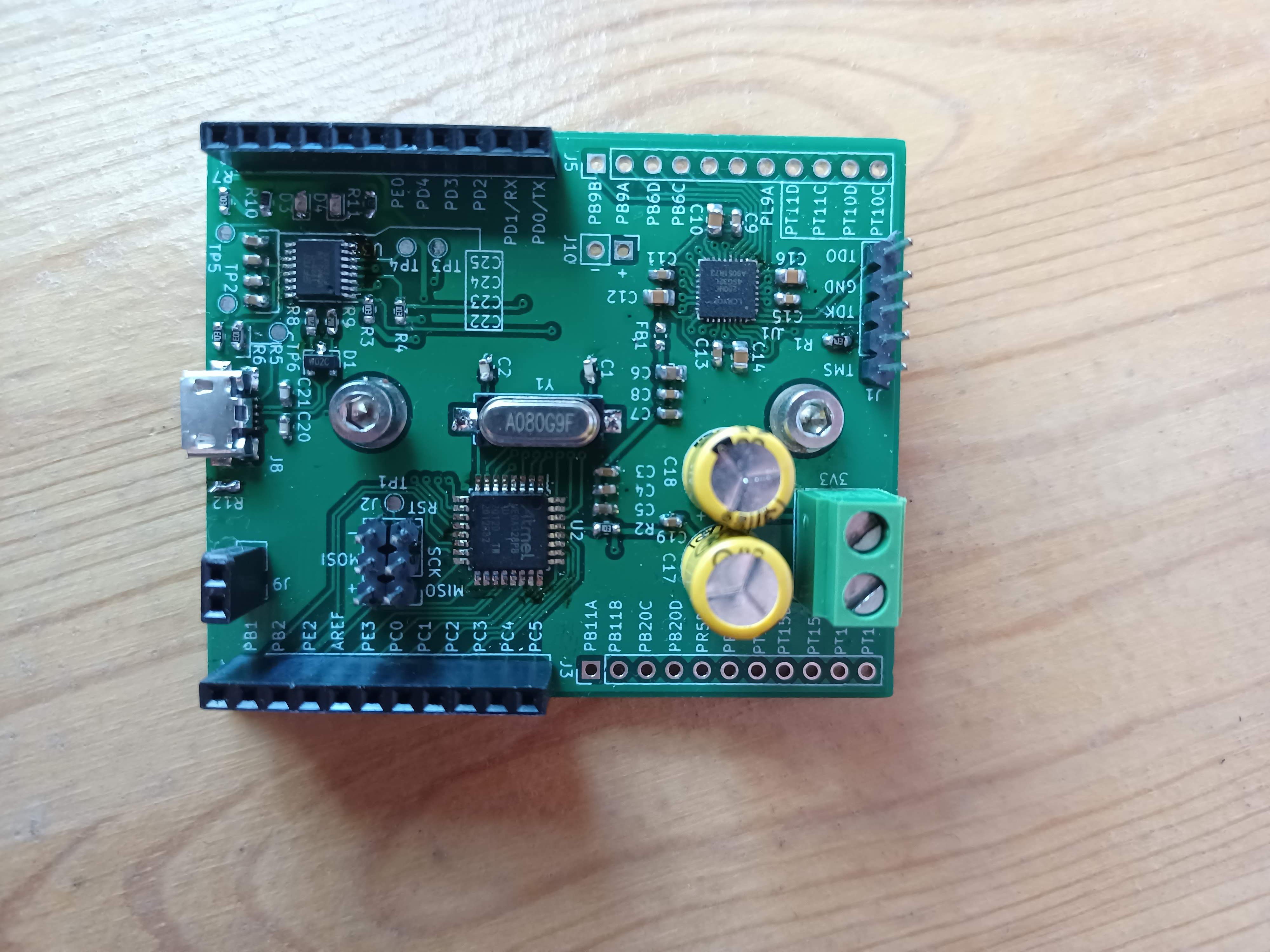
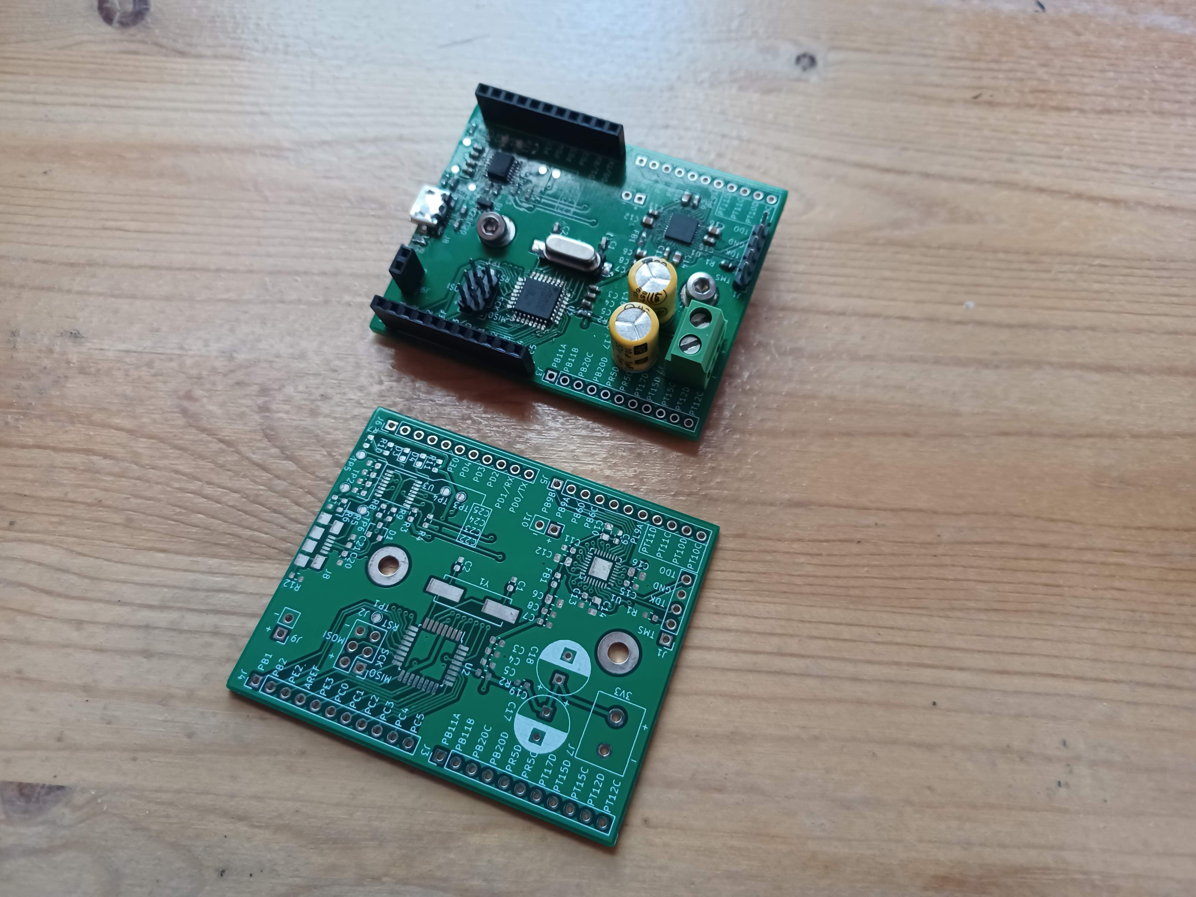
This board was largely a success!
- The ATmega and associated programming circuit all seems to work ok
- Protection on the FTDI part seems to be working (all though you can never really be 100% sure about these things)
- I was able to configure the FPGA
However, there was one big issue... The FPGA kept dying on me. I was able to get two soldered down, and powered up, but after a few minutes they would short out and burn. Before it burned up I was even able to configure one of the FPGAs successfully, which contributes to the mystery.
Further confounding debugging this issue is the current parts shortage. I blew up all of the spare FPGAs I had left over from when I bought parts in 2019, and now they're out of stock everywhere. :(
I tried to check some of the obvious stuff to see if I could figure out a reason that the FPGAs were burning, but I wasn't able to come up with anything
- as far as I can tell the schematic is correct and the board layout is fine
- I checked my power supply's startup for any nasty transient spikes, but was unable to find anything (which doesn't mean they aren't there, but the other chips seem happy, and the FPGA is behind a ferrite bead and a fair amount of smoothing caps)
Unfortunately I wasn't able to check anything else electrical. However, I also had some paranoid Ideas about what could be wrong:
- of the FPGA I had on hand both were originally ordered in 2019 and one had been stored in an opened bag (the micro and ftdi chip were stored in sealed bags), and the other had been soldered to a V1 board, so it possible (but untestable) that poor handling had caused both of the chips to fail somehow
- The other idea that I had was that there was something wrong with the flux I used to solder the FPGA.
I'm specifically suspicious of the flux since its not actually proper electronics flux, its just hardware store plumbing flux. I have used it before on electronics without issue, but the only other time I've used in on stuff this fine pitch was for the V1 board.
you'll recall from the last post That the V1 board suffered from weird intermittent issues with all of the ICs failing randomly (all though I think that the FTDI chip was failing due to poor shielding/transient protection). The same plumbing flux was used on all of those chips, so that's another reason to be concerned.
Since I'd soldered, tested, and burnt out the FPGAs before the rest of the board I decided to just assemble the rest of the board without using the plumbing flux (after carefully cleaning up all of it that I could see on the unpopulated portion of the board). Thus far the non-fluxed circuits seems to be behaving properly.
The evidence against the flux is basically circumstantial, but I'm suspicious anyway.
So This leaves me with a board that works, but absolutely no FPGAs. :(
There are two possible solutions:
- embed the TinyFPGA dev board that I have
- Change to a different FPGA/CPLD that I can still buy
I don't like 1, because I want a project with an embedded FPGA dammit. Therefore I'm pursuing option 2. Either way I'll probably be doing a V4 of the board.
That covers all of the historical background on the electronics for this project, and subsequent posts will describe what's currently happening.
The next post however, will discuss the mechanical design of the device, and show off my fancy new 3d printed case.
Discussions
Become a Hackaday.io Member
Create an account to leave a comment. Already have an account? Log In.