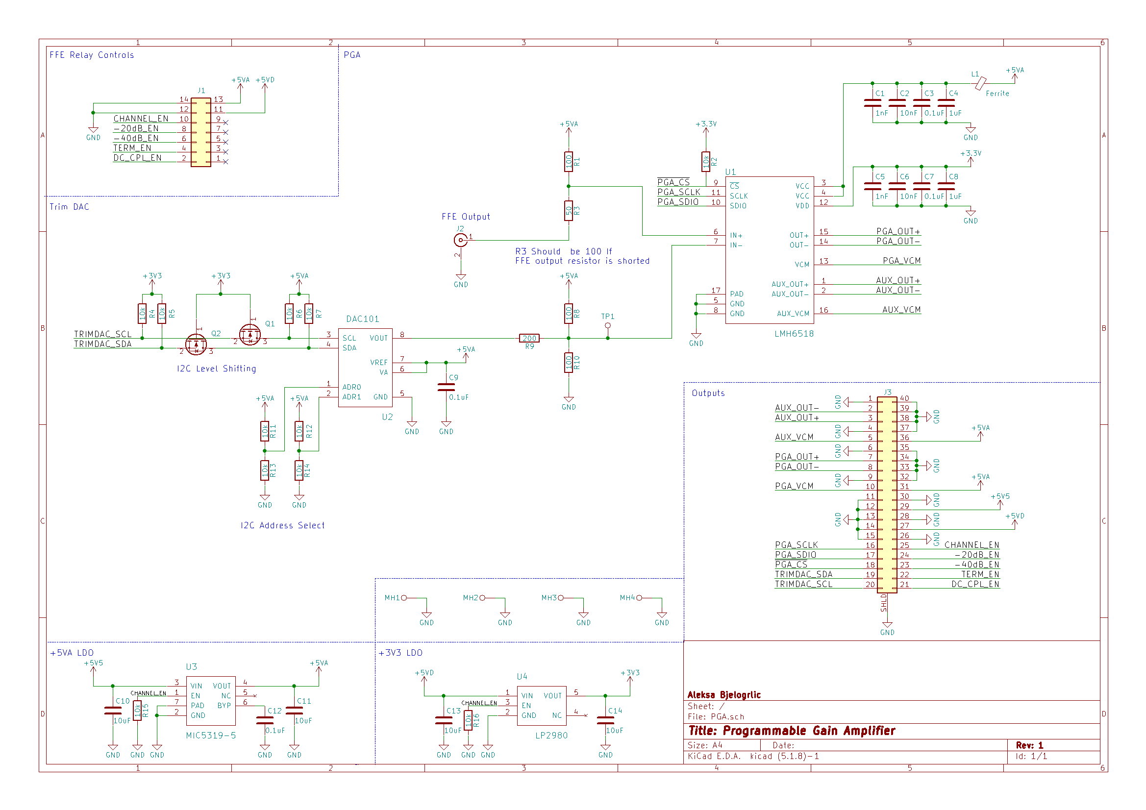
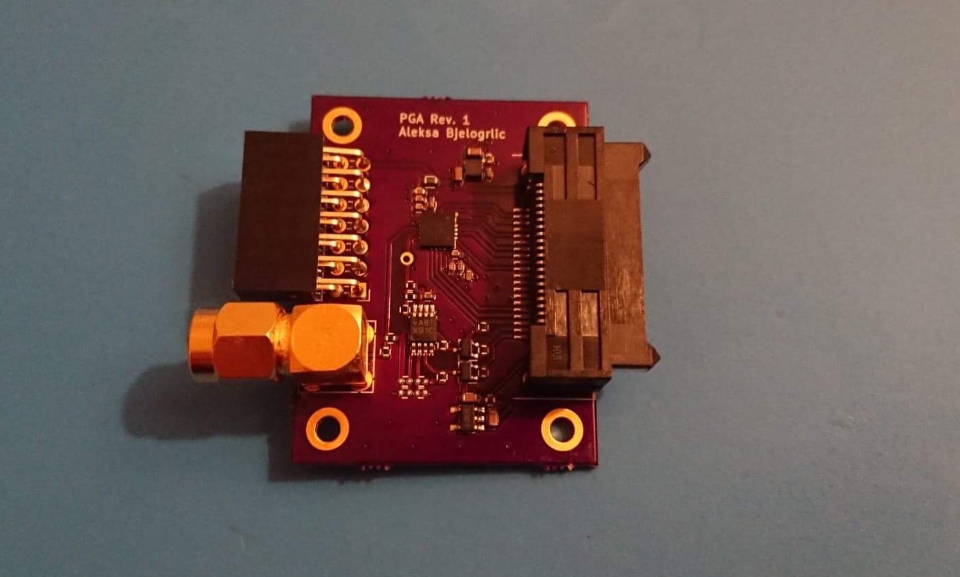
If the FFE is the front of the front end, then what's in the rest of the front end? To complete the front end, this board needed finely adjustable gain, dc offset control, nyquist filtering, and an ADC driver. That sounded like a lot of work! Luckily enough, [bunnie & xobs'] probe schematics introduced me to just the right part for the job, the LMH6518 PGA. With adjustable gain from −1.16 dB to 38.8 dB, a whopping 900 MHz bandwidth, selectable bandwidth limit and 100Ω differential output, this chip had it all!
 To use the input signal from the FFE with this chip, it had to be level shifted from +/-2.5V to 0-5V to fit within the PGA's positive voltage range. This was done by a pair of resistors (at the cost of a 2x attenuation!). DC offset control was accomplished by feeding a DAC output into one end of the PGA. This board also forced me to standardize on a connector series to use for the rest of the prototype. I ended up going with the FX18 series from Hirose, as they were compact (with a reasonably solder-able 0.8mm pitch), rated for high speeds, and had right-angle options that allowed me to connect everything in one plane.
The QFN package gave me some trouble and required rework later, but otherwise this board came together pretty well. I didn't want to continue on with the next board down the line without making sure this chip worked as expected, but probing that connector or its pins would be awful. And so we move on to the topic of the next post, making a front end tester board and testing the front end as a whole!
Thanks for giving this post a read, and feel free to write a comment if anything was unclear or explained poorly, so I can edit and improve the post to make things clearer!
 Aleksa
Discussions
Become a Hackaday.io Member
Create an account to leave a comment. Already have an account? Log In.