Zener Diodes

The Zener diode behaves just like a normal general-purpose diode consisting of a silicon PN junction and when biased in the forward direction, that is Anode positive with respect to its Cathode, it behaves just like a normal signal diode passing the rated current.
However, the Zener Diode or “Breakdown Diode”, as they are sometimes referred too, are basically the same as the standard PN junction diode but they are specially designed to have a low and specified Reverse Breakdown Voltage which takes advantage of any reverse voltage applied to it.
Unlike a conventional diode that blocks any flow of current through itself when reverse biased, that is the Cathode becomes more positive than the Anode, as soon as the reverse voltage reaches a pre-determined value, the Zener diode begins to conduct in the reverse direction.
This is because when the reverse voltage applied across the Zener diode exceeds the rated voltage of the device a process called Avalanche Breakdown occurs in the semiconductor depletion layer and a current starts to flow through the diode to limit this increase in voltage.
The current now flowing through the Zener diode increases dramatically to the maximum circuit value (which is usually limited by a series resistor) and once achieved, this reverse saturation current remains fairly constant over a wide range of reverse voltages. The voltage point at which the voltage across the Zener diode becomes stable is called the “Zener voltage”, ( Vz ) and for Zener diodes, this voltage can range from less than one volt to a few hundred volts.
The point at which the Zener voltage triggers the current to flow through the diode can be very accurately controlled (to less than 1% tolerance) in the doping stage of the diodes semiconductor construction giving the diode a specific Zener breakdown voltage, (Vz) for example, 4.3V or 7.5V. This Zener breakdown voltage on the I-V curve is almost a vertical straight line.
Disadvantages of Zener Voltage Regulator:
- It has poor efficiency for heavy loads because a considerable amount of power is wasted in Zener resistance (
R2) and series resistor (RS) in comparison with load power. - The DC output voltage slightly changes due to Zener resistance.
Linear Voltage Regulator

Linear voltage regulators—also called LDOs or low-dropout linear regulators—use a transistor controlled by a negative-feedback circuit to produce a specified output voltage that remains stable despite variations in load current and input voltage.
A basic, fixed-output-voltage linear regulator is a three-terminal device. Some linear regulators allow you to adjust the output voltage by means of an external resistor.
The disadvantage of Linear Voltage Regulator
A serious disadvantage of linear regulators is their low efficiency in many applications. The transistor inside the regulator, which is connected between the input and output terminals, functions as a variable series resistance; thus, high input-to-output voltage differential combined with high load current results in large amounts of power dissipation. The current required for the functionality of the regulator’s internal circuitry, labelled IGND in the diagram, also contributes to total power dissipation.
Perhaps the most likely failure mode in a linear-regulator circuit derives from thermal rather than strictly electrical factors.
DC-DC Buck Converter

A buck converter (step-down converter) is a DC-to-DC power converter that steps down voltage (while stepping up current) from its input (supply) to its output (load). It is a class of switched-mode power supply (SMPS) typically containing at least two semiconductors (a diode and a transistor, although modern buck converters frequently replace the diode with a second transistor used for synchronous rectification) and at least one energy storage element, a capacitor, inductor, or the two in combination. To reduce voltage ripple, filters made of capacitors (sometimes in combination with inductors) are normally added to such a converter's output (load-side filter) and input (supply-side filter).
You can read more about buck converters here.
Advantage of DC-DC Buck Converter
- The efficiency of the Buck regulator is about 90%.
- The cost and size are low.
- Line voltage variation has large tolerance.
How to make a DC-DC Buck Converter?

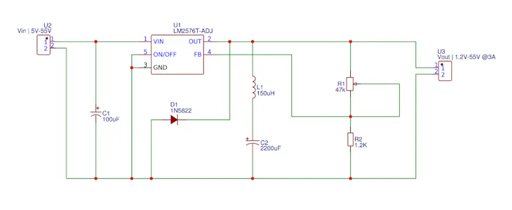
With LM2576T-ADJ, we have feedback and the output will stay the same using different loads. Just make the connections, add the input capacitor to have a steady input and you're done.
The input could be in the range of 5 to 55 volts. Don't apply a higher voltage or you could burn the LM2576T-ADJ component. In this case, we need no external switch since the LM2576T-ADJ already has it inside it. With the feedback pin connected to the output voltage divider, the LM2576T-ADJ will change the width of the pulse depending on the output in order to keep it constant. In this case, use a Schottky Barrier Rectifier diode because it has a low forward voltage. This diode will live the current flow when the switch is open.
Putting all the stuff together

Follow the below steps to assemble the device at home easily:
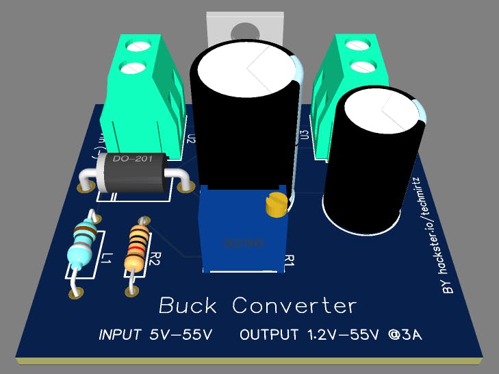
- Download the Gerber files for the PCB from here or down below.
- Go to PCBWay.com and upload the files get your PCBs at home at a very low price. Also, you can get a $5 Welcome Bonus. They are the most cost-effective and quality-oriented PCB manufacturers. You can order your prototype PCBs in a small quantity, as small as 5 pcs of PCB. In addition to the standard PCBs, we could also support advanced PCBs, FPC/rigid-flex PCBs and other related services.
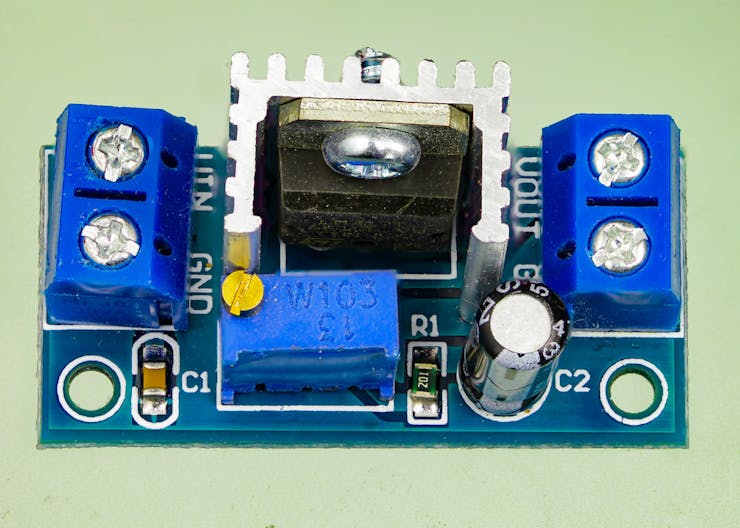
- Solder the components on the PCB as per the schematic and design shown below.
- Connect the input power supply(DC) in the input terminals and using a multimeter, adjust the output voltage by adjusting the screw on the potentiometer.