 agp.cooper
Reworking the existing Flash ROM programmer
A new PCB is coming that allows programming of larger capacity Flash ROM chips than the AT29C256. But it makes an excellent test bed for the firmware.
Here are the first and second generation Flash ROM programmers:
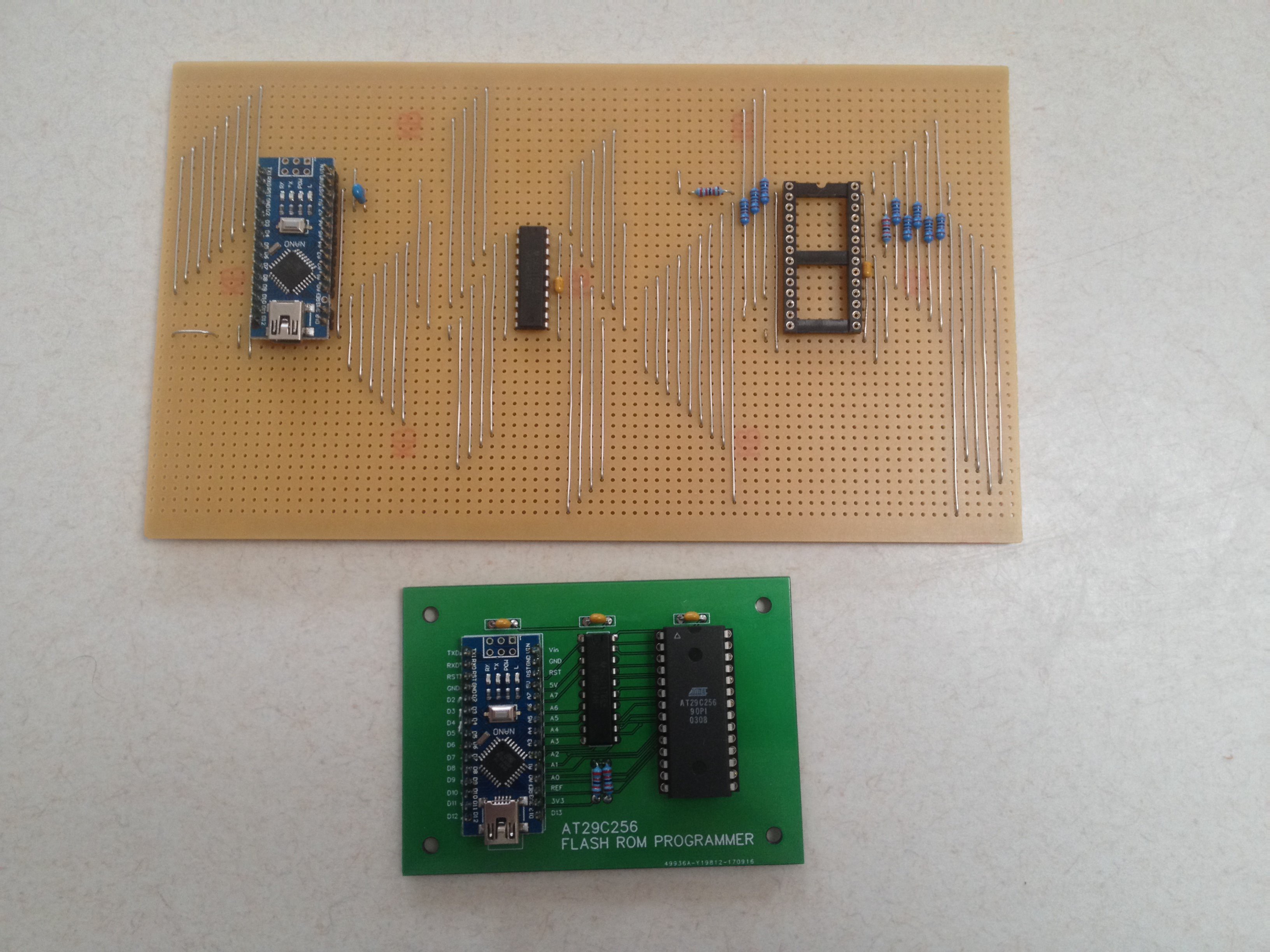
These programmers can only address 32x8kb in software. With two address latches (i.e. 74HC374) the address space expands to 512x8kb (or more).
HEX8-16 Support
The firmware interprets HEX8, line types 0 (data) and 1 (end of file), and the Hex16 line type 2 (extended segment address). Hex16 line type 3 (start segment address) is not supported. Using line type 2 allows access to 1M of address space.
Multiple hex files can be include in the upload file and files can be shifted (if appropriate) using line type 2.
Options
At the moment the firmware only support the AT29C256 but the plan is to support on the fly parameters for ROM size, Page size, Software Date Protection and Boot Lockouts.
Upload speed
Really there is no reason to upload data faster/slower than 9600 baud. No handshaking is required.
Schematic
Here is the new schematic. The current firmware is not compatible due to design changes:
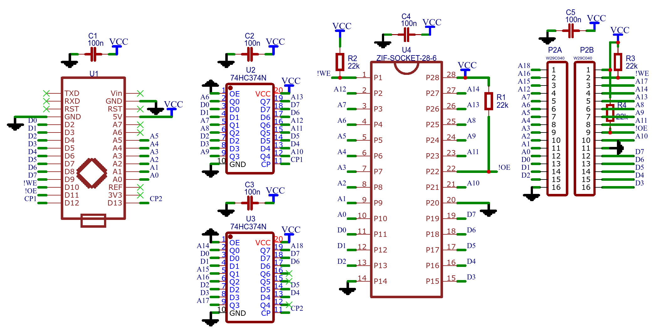
Looking at the schematic now, I see a small error. A18 attaches to D7 rather than D4. No matter I can fix it if there is a new generation.
AlanX
Discussions
Become a Hackaday.io Member
Create an account to leave a comment. Already have an account? Log In.