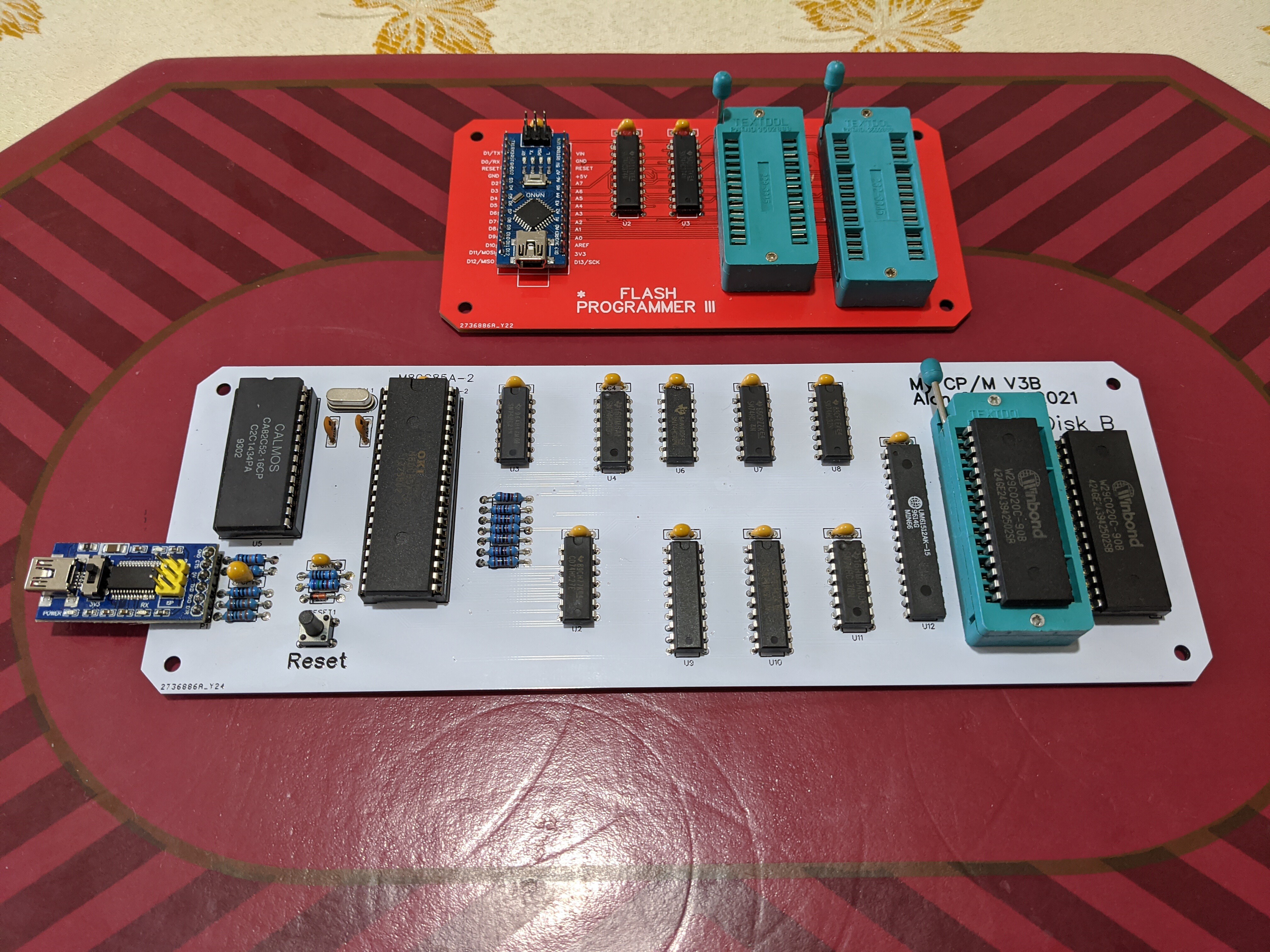
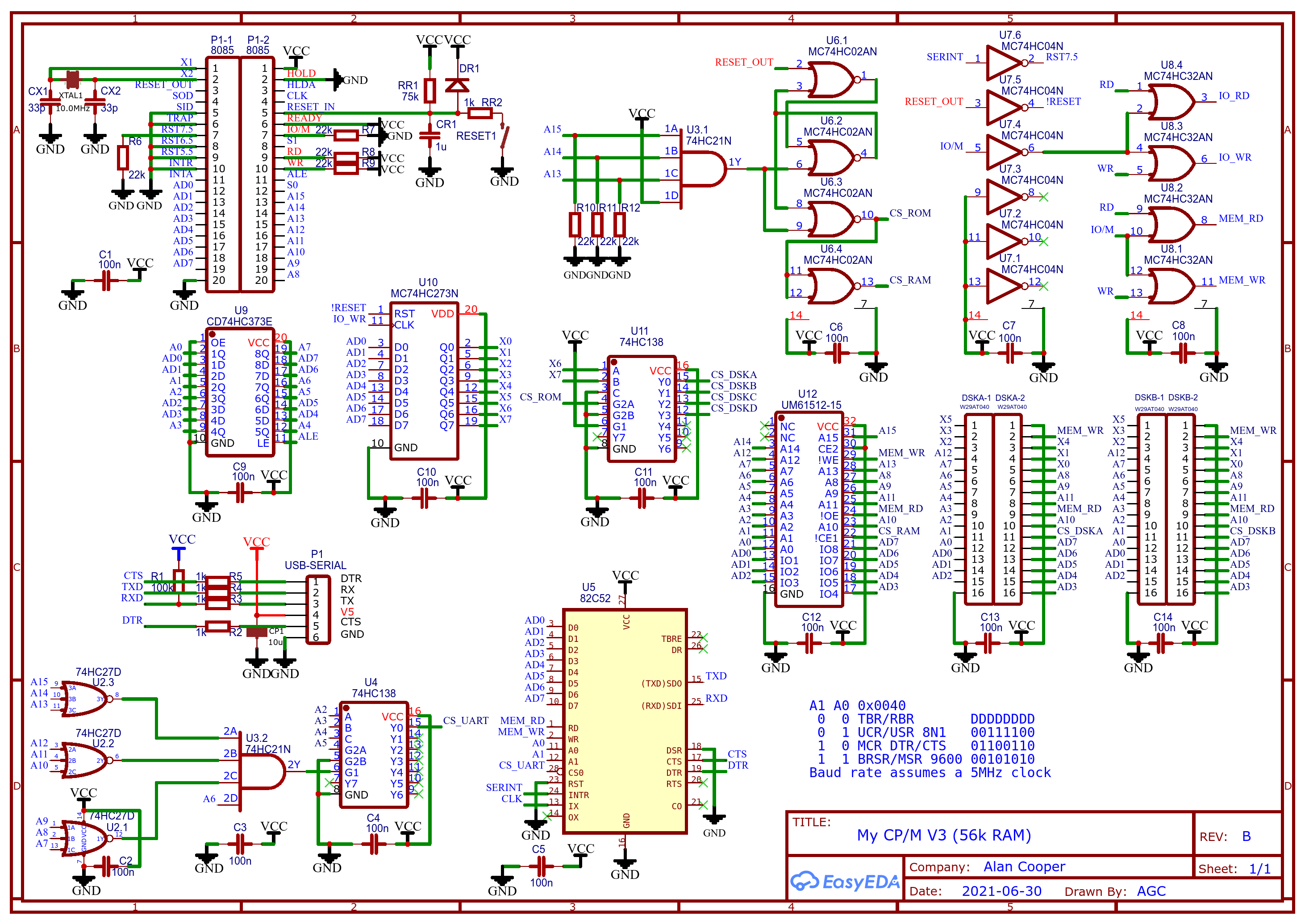
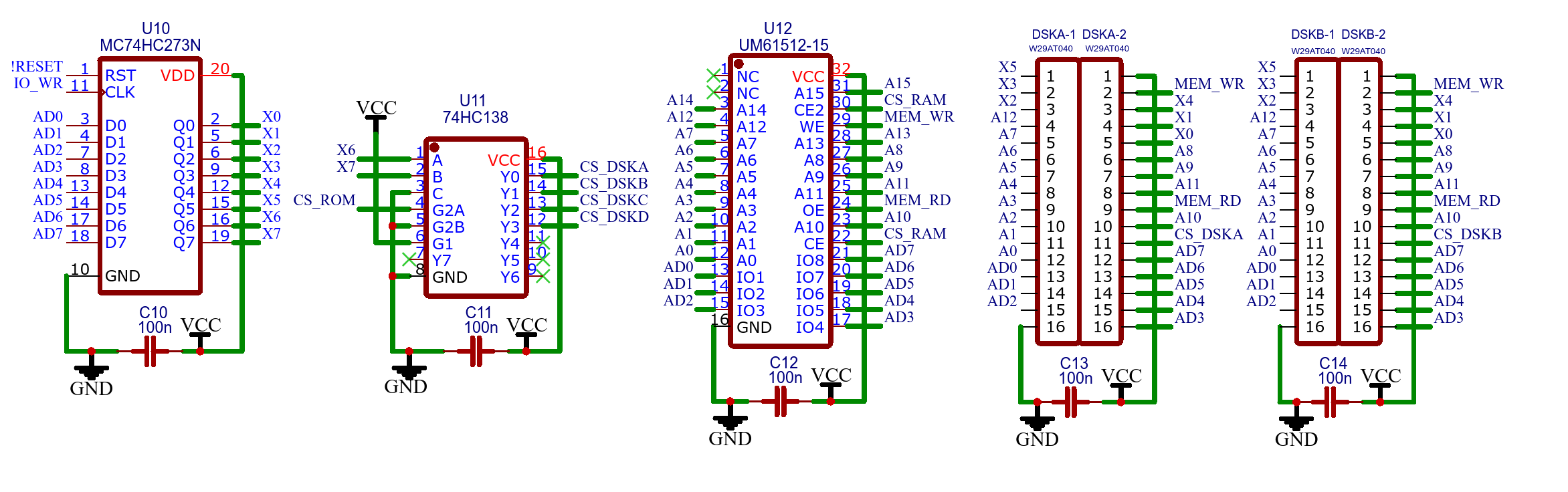
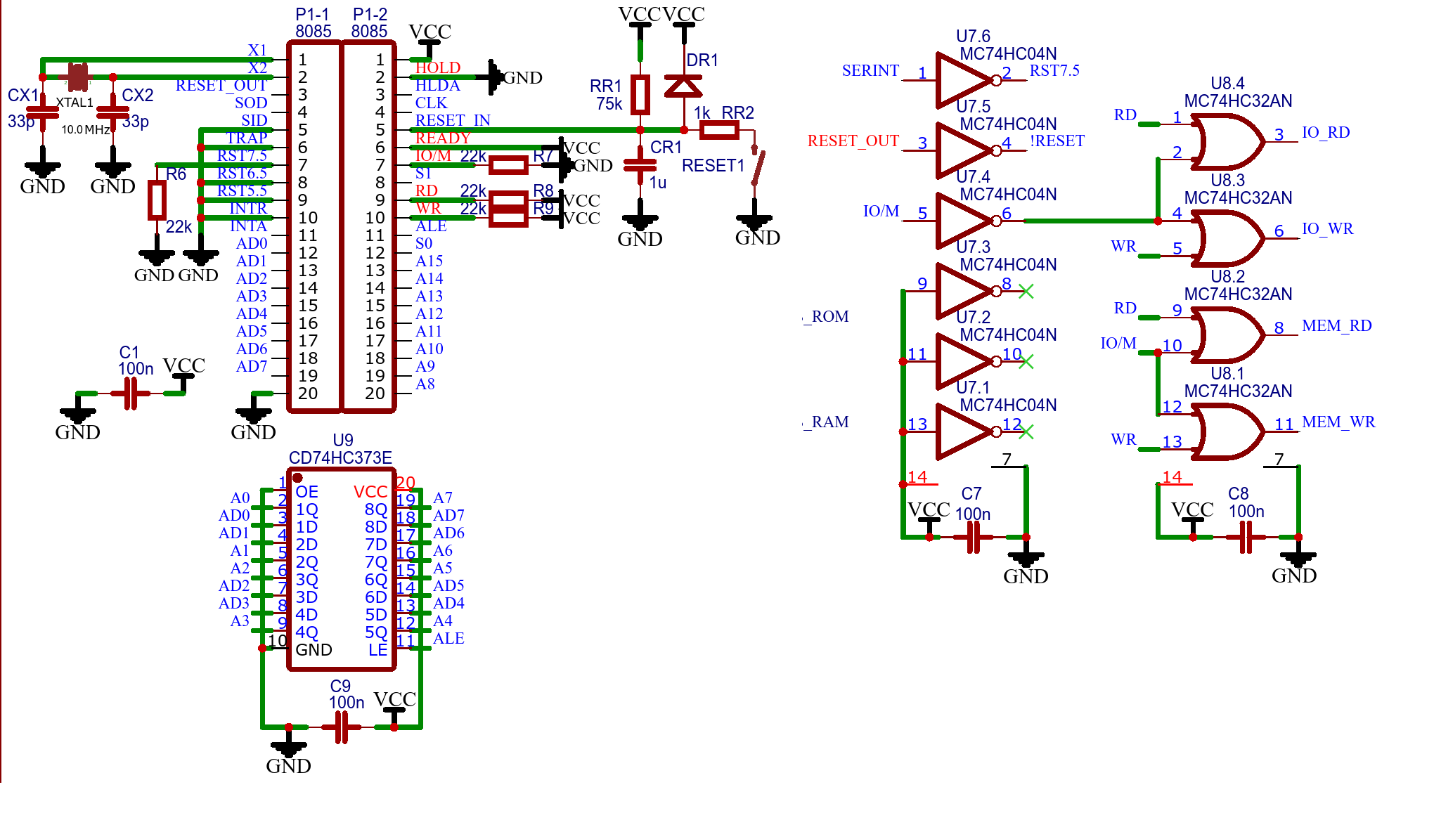
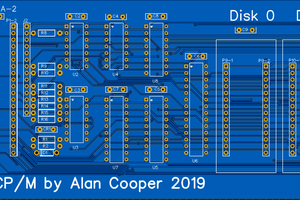
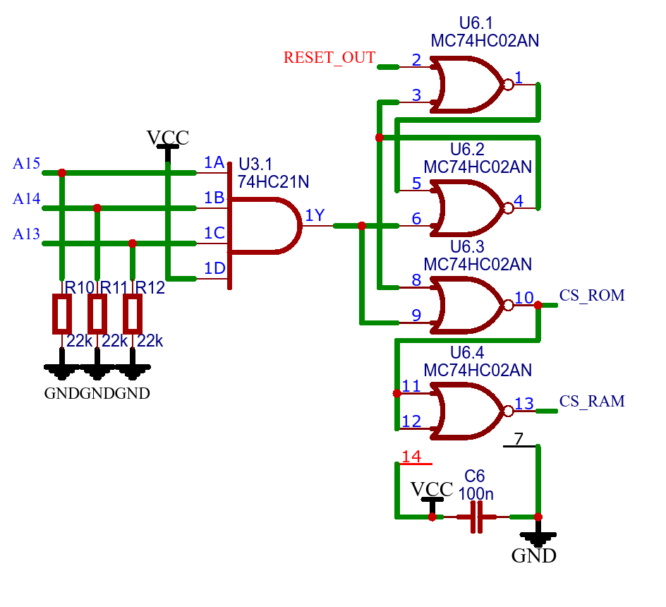
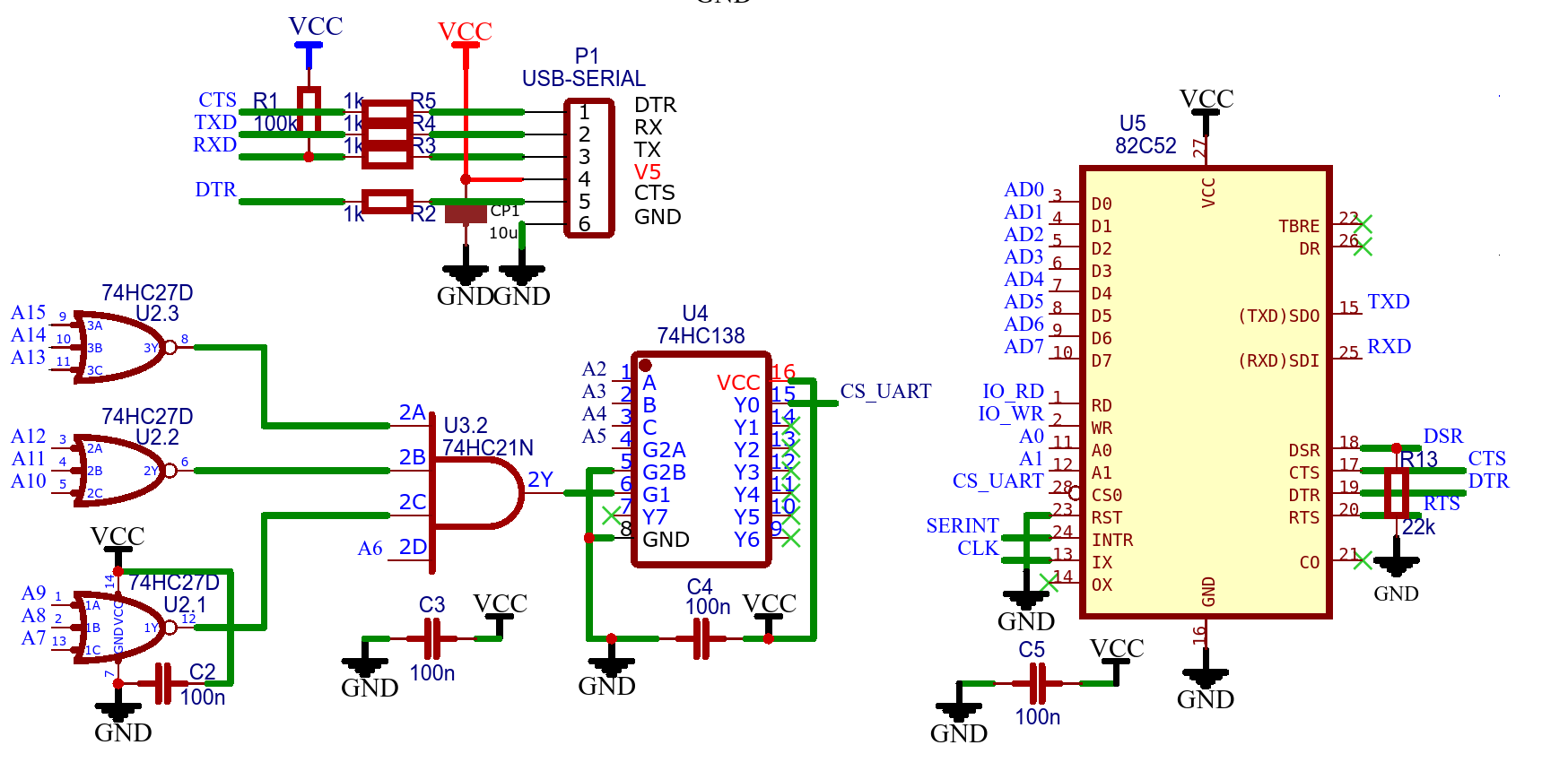
Version 3 of My CP/M uses an UART (rather than firmware serial) and 256kb or 512kb Flash ROM chips as disks
To make the experience fit your profile, pick a username and tell us what interests you.
We found and based on your interests.
CPM_2_0_Interface_Guide.pdfAdobe Portable Document Format - 3.78 MB - 07/02/2021 at 03:15 |
|
|
Intel 8080-8085 Assembly Language Programming 1977 Intel.pdfAdobe Portable Document Format - 5.51 MB - 07/02/2021 at 03:15 |
|
|
CPM_2.2_Alteration_Guide_1979.pdfAdobe Portable Document Format - 3.69 MB - 07/02/2021 at 03:14 |
|
|
Schematic_my CP_M V3B_2021-07-02.pngPortable Network Graphics (PNG) - 822.71 kB - 07/02/2021 at 03:14 |
|
|
CPM_2_0_System_Alteration_Guide.pdfAdobe Portable Document Format - 3.36 MB - 07/02/2021 at 03:14 |
|
|
Updated Boot
First I have to update boot.asm, the code to load CP/M into memory. The CP/M V2 only had 32kb of RAM so the CP/M source was located at 0x8000. As CP/M V3 has 56k of RAM so the CP/M source is located at 0xE000.
Here is the boot assembly code (i8085):
; boot.asm: Load CP/M from ROM ; Calc CPM addresses msize equ 56 ; 56k RAM sectors equ 16 ; sectors per track for my system systrks equ 4 ; my boot system has 4 tracks of 16 sectors bias equ (msize-20-1)*1024 ; calculation for my system ccp equ 3400h+bias cstart equ 4a00h+bias org 0e000h ; executed in ROM after shift down jmp 0e003h ; reset bootstrap boot: di ; disable interrupts lxi sp,ccp-0080h ; convenient place lxi d,ccp-0080h ; start of boot dst lxi h,0e000h ; start of ROM (boot src) mvi c,sectors ; sectors per track mvi b,systrks ; sytem track count push b ; save boot$nextsect: mvi b,128 ; sector size boot$copysect: mov a,m inx h stax d inx d dcr b jnz boot$copysect dcr c jnz boot$nextsect pop b dcr b push b jnz boot$nextsect ; Cold boot jmp cstart end
Updated CBIOS
CBIOS has a number of alterations to suit the new hardware design:
; Calc CPM addresses msize equ 56 ; RAM capacity sectors equ 16 ; sectors per track for my system systrks equ 4 ; my boot system has 4 tracks of 16 sectors bias equ (msize-20-1)*1024 ; adjusted for my system cbase equ 3400h+bias ; base of ccp fbase equ cbase+800h ; base of bdos bdos equ cbase+806h ; bdos entry cbios equ cbase+1600h ; base of custom bios (cold boot entry) spbase equ msize*1024 ; sp base (use top of RAM) usrdsk equ 0004h ; current user and disk number iobyte equ 0003h ; intel i/o byte rst7.5 equ 003ch ; interrupt to read serial data input lf equ 0ah ; line feed cr equ 0dh ; carriage return ; Custom CP/M 2.2 BIOS org cbios ; jump vector for individual subroutines jmp cboot ; cold start wstart: jmp wboot ; warm start jmp const ; console status jmp conin ; console character in jmp conout ; console character out jmp list ; list character out jmp punch ; punch character out jmp reader ; reader character out jmp home ; move head to home position jmp seldsk ; select disk jmp settrk ; set track number jmp setsec ; set sector number jmp setdma ; set dma address jmp read ; read disk jmp write ; write disk jmp listst ; return list status jmp sectran ; sector translate ; System uses a two Flash AT29C020-90B with 2048 x 128b pages (256k) ; Set as 128 tracks of 16 sectors of 128 bytes ; System uses tracks 0 to 3 (64 sectors) ; Directory is track 4 and 7 (128 entries) ; Leaving 240kb file storage using 2048b blocks per chip dpbase: ; disk Parameter header for disk A (system) dw trans, 0000h dw 0000h, 0000h dw dirbf, dpblk256s dw chk00, all00 ; disk parameter header for disk B (system) dw trans, 0000h dw 0000h, 0000h dw dirbf, dpblk256s dw chk01, all01; ; disk parameter header for disk C (data) - Not installed dw trans, 0000h dw 0000h, 0000h dw dirbf, dpblk256d dw chk02, all02 ; disk parameter header for disk D (data) - Not installed dw trans, 0000h dw 0000h, 0000h dw dirbf, dpblk256d dw chk03, all03 ; sector translate vector (i.e. no translation) trans: db 1, 2, 3, 4 ; sectors 1, 2, 3, 4 db 5, 6, 7, 8 ; sectors 5, 6, 7, 6 db 9, 10, 11, 12 ; sectors 9, 10, 11, 12 db 13, 14, 15, 16 ; sectors 13, 14, 15, 16 ; disk parameter block for system disk (256k) and 1k block size dpblk256s: dw sectors ; SPT: sectors per track db 3 ; BSH: block shift factor db 7 ; BLM: block mask db 0 ; EXM: extended block mask dw 247 ; DSM: disk blocks - 1 dw 127 ; DRM: directory max - 1 db 240 ; AL0: alloc 0 (=4 bits) db 0 ; AL1: alloc 1 dw 0 ; CKS: check size (= not removable) dw systrks ; OFF: track offset ; disk parameter block for data disk (256k) and 1k block size dpblk256d: dw sectors ; SPT: sectors per track db 3 ; BSH: block shift factor db 7 ; BLM: block mask db 0 ; EXM: extended block mask dw 255 ; DSM: disk blocks - 1 dw 127 ; DRM: directory...Read more »
Assembled
The 74HC21's arrived today. Here is the assembled machine:
Hopefully for schematic mistakes.
Next to do is to update the CBIOS for the 82C52 SIO.
TBC ...
AlanX
Final Check
I checked as much as I could. Particularly the 82C52 as it is new. Changed IO_RD/IO_WR to MEM_RD/MEM_WR (that would make the board useless).
Updated the crystal frequency to 10MHz.
So now I just have to wait a week or so for the PCB to arrive.
Final Schematic:
As much as I try I still find errors after sending the PCB to be manufactured.
I updated the labels on UM61512 to make it clearer but I connected CE2 to CS_RAM rather than VCC. No matter, I can patch the board.
AlanX
Disk Access
Disk access uses the 8kb address space above the top of RAM. The 8kb window is mapped to the disk space with a write to I/O. Left over map space is used to select up to four disks:
Although the method is fast it costs 8kb of RAM (i.e. 56kb rather than 64kb of RAM). After boot up it is not necessary to have ROM in the address space. I should look at this again later.
AlanX
The CPU Schematic
Here is the schematic:
Nothing really unique here. Typical address bus decoding (IC9) and IO/MEM RD/WR.
AlanX
CP/M Boot Logic
One the things about CP/M is that upon reset the system boot from ROM. The ROM loads the CP/M operating system. For the i8085, reset starts at address 0x0000. In normal operation CP/M expects everything to be RAM. The zero page (0x0000 to 0x00FF) is used by CP/M and programs are loaded from 0x0100 up. And CP/M lives at the TOP of RAM.
Therefore some logic is needed to move the boot system ROM address to 0x0000 on system reset. After boot/reset the address logic needs to be set for access to normal RAM.
This can be done with a Set/Reset Latch using IC3 and IC6. On system reset, RESET_OUT set the latch, and A15, A14 and A13 reset the latch. Normally, the address of CS_ROM is 0xF800 to 0xFFFF (8kb) and the address of CS_RAM is 0x0000 to 0XF7FF (56kb). On system reset the latch is set and CS_ROM is set/locked low and CS_RAM is set/locked high. A high address (0xF800 to 0xFFFF) reset the latch to normal use.
One of the advantages of the system is that 8kb the ROM is visible above memory. This makes access to ROM fast. The down side is less RAM.
Other methods
Grant Searle uses I/O to set and reset the boot ROM. After boot he access the harddisk via I/O. Therefore his system has 64kb or RAM.
I am leaning towards Grant's banked memory approach, and using "port" (i.e. I/O or memory mapped) to access hardware.
I have already decoded 4x4 ports starting at 0x0040 (e.g. the UART).
But let us use baby sets!
AlanX
The 82C52 UART
The 82C52 is a single channel UART. Here is my schematic:
It is quite adaptable to different clock frequencies. Using the M80C85A-2 clock of 5 MHz (i.e the maximum recommended clock speed), here are the available baud rates:
Note: A 9.8304 MHz crystal would make these baud rates exact.
Going through my crystal junk box I find an 11.0592 MHz crystal. I could use this directly on the 82C52 and get a large range of exact bauds:
Anyway I will stay with the 10MHz crystal for the M80C85A-2.
Programming the 82C52
I have fully decoded an address of 0x0040 (i.e. 0x40-0x43) which in reserved for the CBIOS in the zero page. I guess it is not often used as it takes some effort to decode.
Here are the initialisation codes for 9600 8N1:
The decoding scheme can be used for up to to 3 other devices using the CBIOS reserved area.
AlanX
Create an account to leave a comment. Already have an account? Log In.
Become a member to follow this project and never miss any updates