 agp.cooper
The CPU Schematic
Here is the schematic:
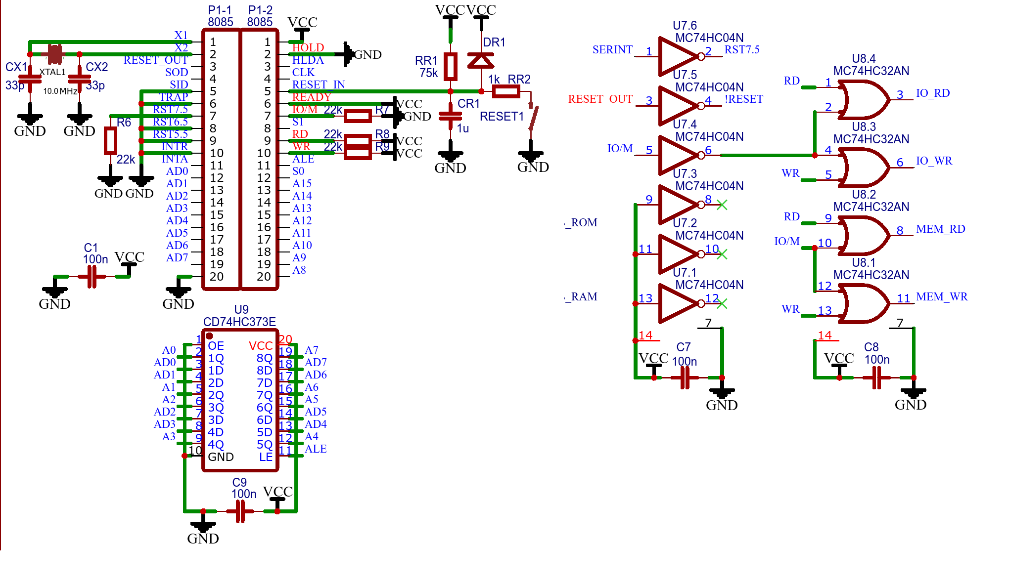
Nothing really unique here. Typical address bus decoding (IC9) and IO/MEM RD/WR.
AlanX
A project log for My CP/M V3
Version 3 of My CP/M uses an UART (rather than firmware serial) and 256kb or 512kb Flash ROM chips as disks
The CPU Schematic
Here is the schematic:
Nothing really unique here. Typical address bus decoding (IC9) and IO/MEM RD/WR.
AlanX
Discussions
Become a Hackaday.io Member
Create an account to leave a comment. Already have an account? Log In.