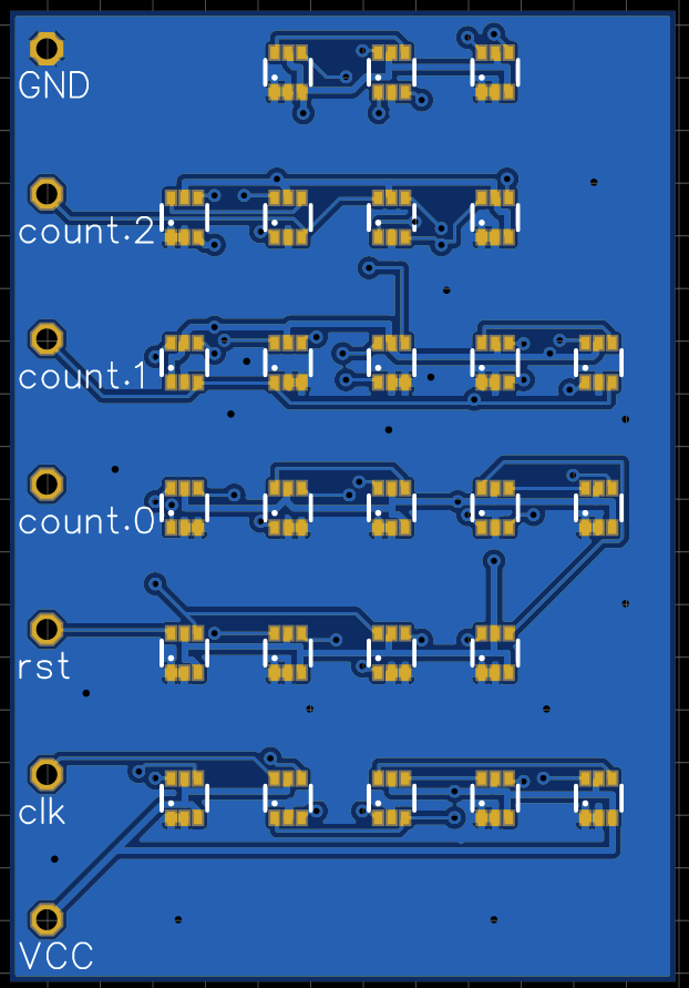
The flow is, of course, not limited to resistor-transistor-logik. In the meantime, I implemented analog multiplexer logic and already received a first PCB with the counter implemented in that logic style. The generated PCB is shown below. The analog multiplexers (BL1551) come in a tiny SC70 package and leave ample space for routing. The implementation of logic gates with multiplexers is quite efficient, hence only 26 devices are needed.

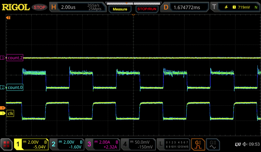
Unfortunately something turned out to be not quite right with the circuit. The scope image below shows the clock signal after the first inverter (count.0). This seems to work well, but the "high" state is unusually noisy, suggesting that something is oscillating and contaminating the supply rail.

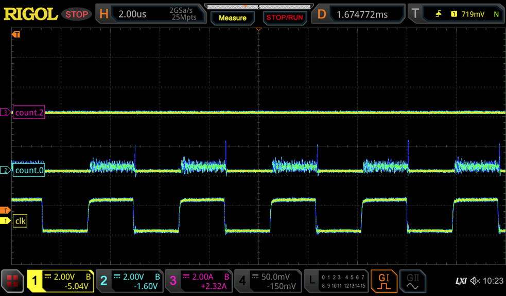
Debugging things a bit further, I isolated one of the latches. Seems that the latch does not really save the input state, but does instead alter between "low" and "oscillating".

Turns out that there is indeed something wrong with the PCB. Instead of closing the latch with positive feedback, I accidentally swapped polarities of the buffer so that there is negative feedback. A nice oscillator indeed, and not a working digital circuit
Microcells, introducing post layout extraction
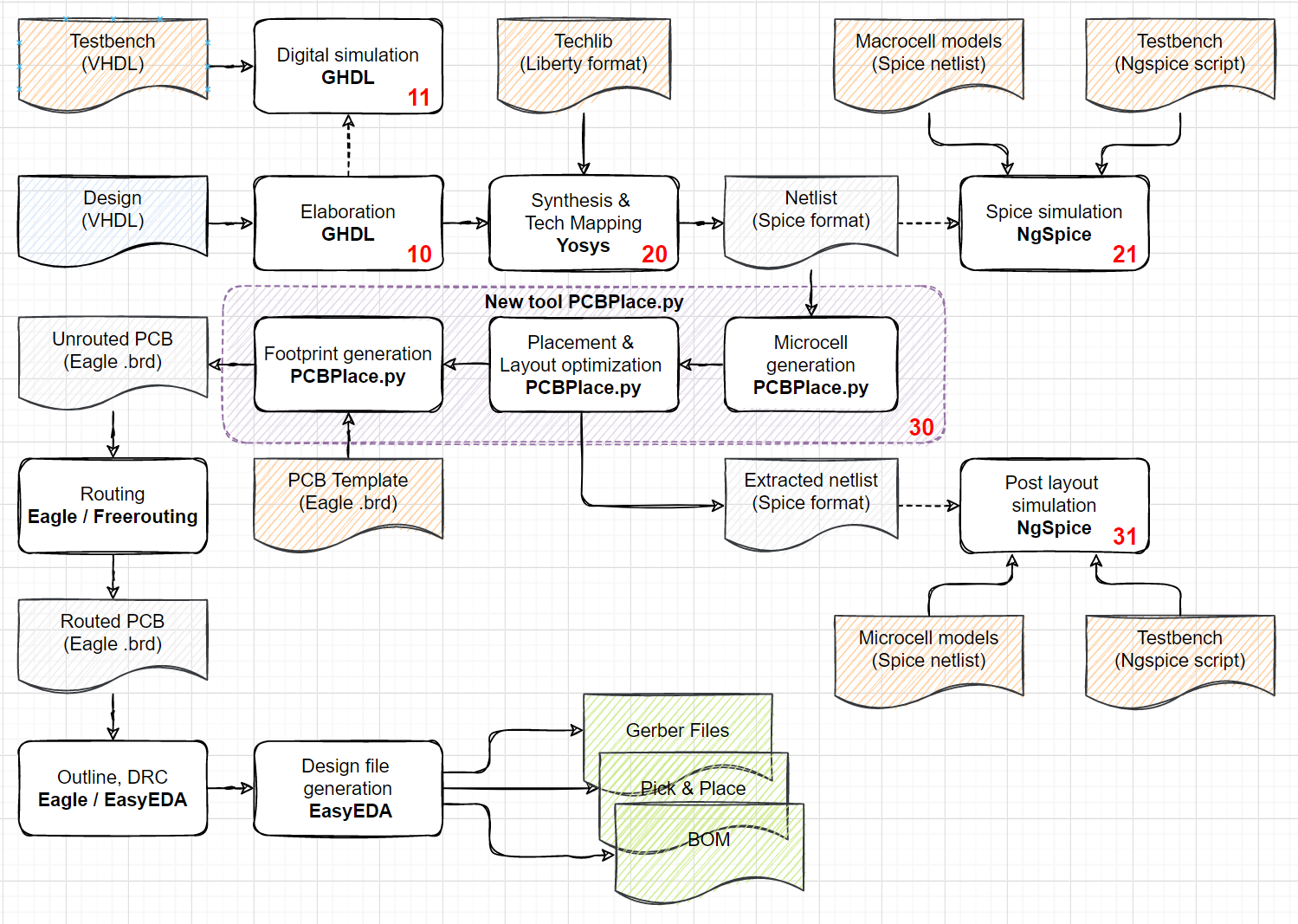
So what went wrong here? I did indeed skip a step in my earlier description of the flow. The problem is that Yosys does not really know about analog multiplexers or transistors. Hence I introduced a step between Yosys and the actual placement of the components on the PCB. Yosys/GHDL is generating basic logic gates as output (e.g. NAND, NOR). The first pass of my PCBPlace.py tool is to break down these gates into "Microcells", the actual components that are being placed on the PCB. In this case, between 1 and 5 analog multiplexers are generated per gate. Turns out I made a mistake that was difficult to spot in the microcell implementation of the latch. The only way to detect this, would have been to manually retrace the PCB layout.
To address this "loophole", I introduced another feature to the flow, the post layout extraction.

The image above shows the updated flow with the step of microcell generation being made more visible. The PCBPlace.py tool will now automatically extract a spice netlist after microcell generation, placement and layout optimization. The extracted netlist can then be simulated (Script 31) with NgSpice to spot any errors in microcell generating or during subsequent optimization steps.
Off to the next round of verification PCB builds. My plan is to have a second round with simpler circuits and then head for a full CPU build as a third step.
 Tim
Tim
Discussions
Become a Hackaday.io Member
Create an account to leave a comment. Already have an account? Log In.