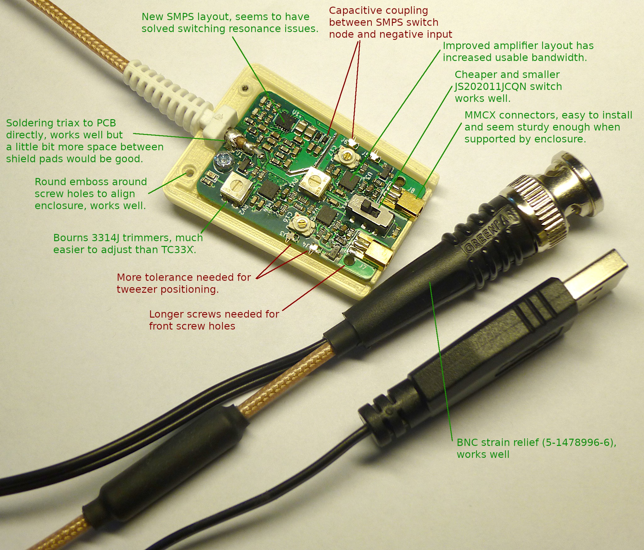
I received the revision 4 PCBs last week and have assembled one prototype. I already hoped that I wouldn't find anything more to improve, but that doesn't seem to be the case. Normally at this point a boss would say "it's good enough, wrap it up" - but my current boss (myself) is very bad at knowing when to stop.

Biggest letdown is the return of SMPS noise. Not conducted noise, mind you, but capacitively coupled noise. In relayouting the SMPS section and adjusting the frontend layout, I ended up moving the negative input spring terminal too close to the switching node of the SMPS. This causes a few mV amplitude square wave to appear, especially when probes are floating. The fix should be simple enough, moving the parts around a bit so that the capacitors will better shield the terminal. Though there is an alternative of just installing a bit of copper tape as a shield manually.
When ordering the PCBs, I had to make a last minute change to the design because the parts next to MMCX connector were too narrow to manufacture. As a consequence, the front screws now go all the way through the PCB, and the 8 mm long screws do not have enough plastic to hold well. It will be a simple matter of switching to 10 mm screws and adjusting the enclosure design to have through holes for them.
Finally, for some reason, I seem to have even worse tolerance for the tweezer tip fitting in the 3D printed enclosure than before. But thanks to the PCB change, there is now much more space for the ground spring contact up front, so it would be possible to adjust the layout to make it more tolerant of enclosure inaccuracies.
Overall, I think my perfectionism will require a revision 5. But the changes are getting smaller, so hopefully if I test this prototype well, the next version is something I can call "final" and start manufacturing.
 Petteri Aimonen
Discussions
Become a Hackaday.io Member
Create an account to leave a comment. Already have an account? Log In.