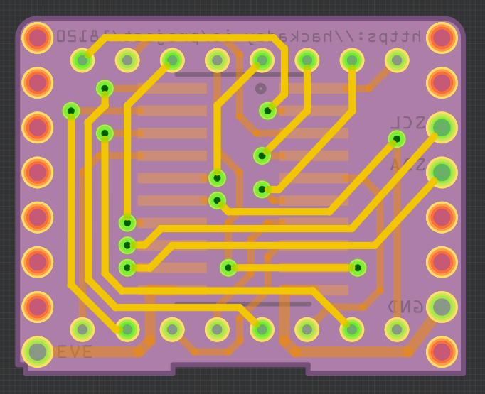
n other news, now that I actually know the pin spacing of those matrices, I re-did the PCB design, taking that into account, and also moving the chip on the underside, so that the whole thing is not as thick.

It's no longer a 1" square, since the different positioning of the chip, generous sprinkling of vias and extra space at the edges left me enough room for all the traces.
 deʃhipu
Discussions
Become a Hackaday.io Member
Create an account to leave a comment. Already have an account? Log In.