 Making Devices
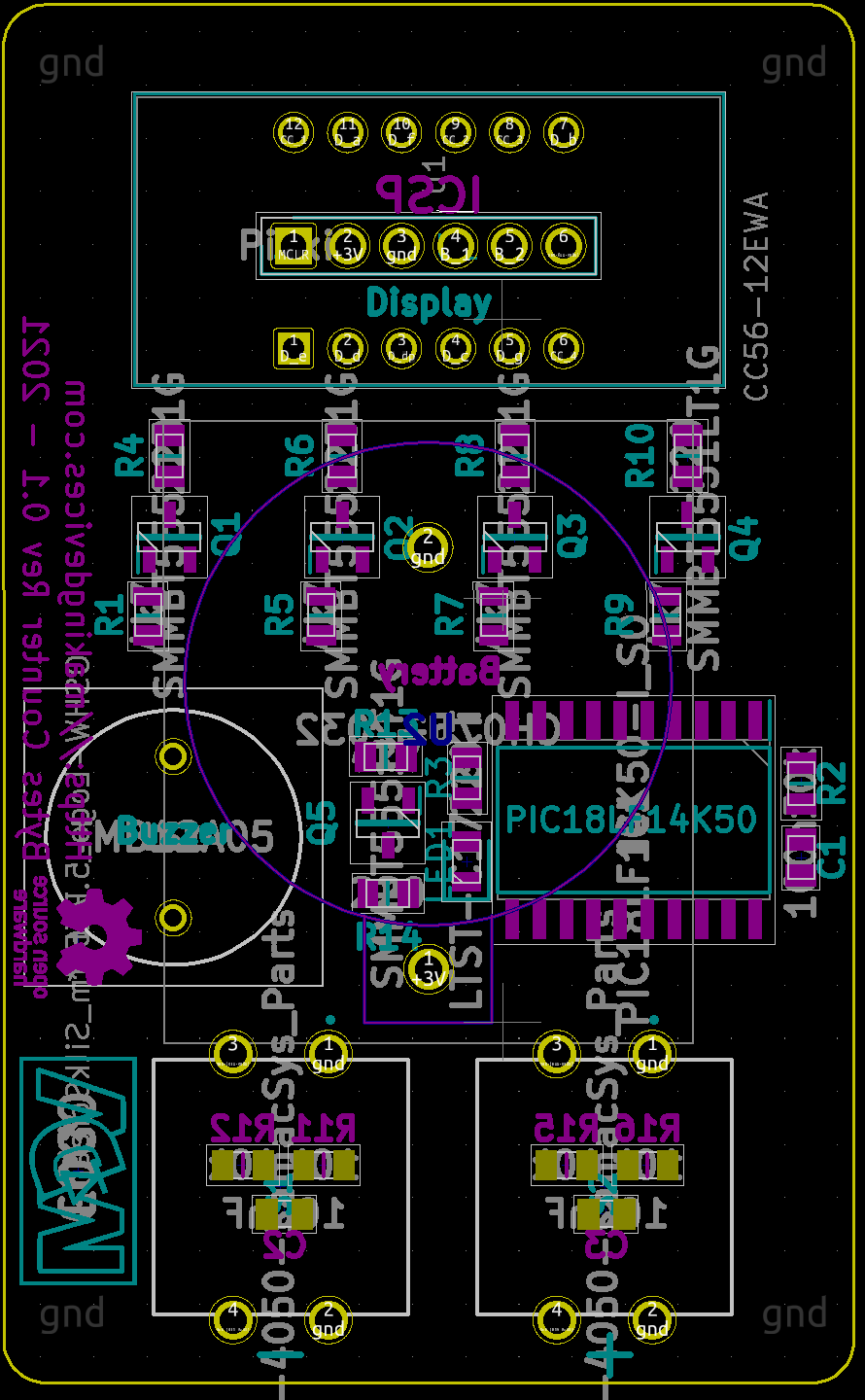
Components are placed, trying to use the fewer space possible in a 2-layer PCB:
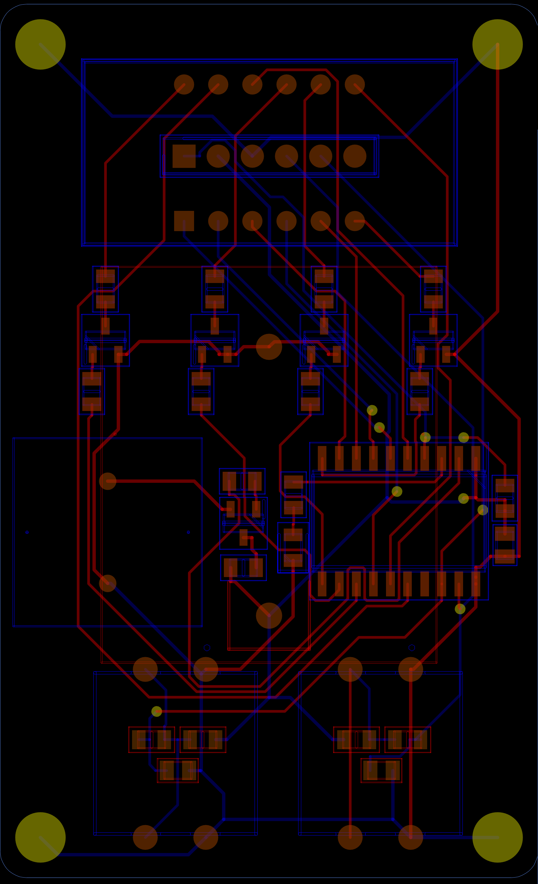
Then, exporting the files from Kicad to FreeRouting tool, the layor is made:
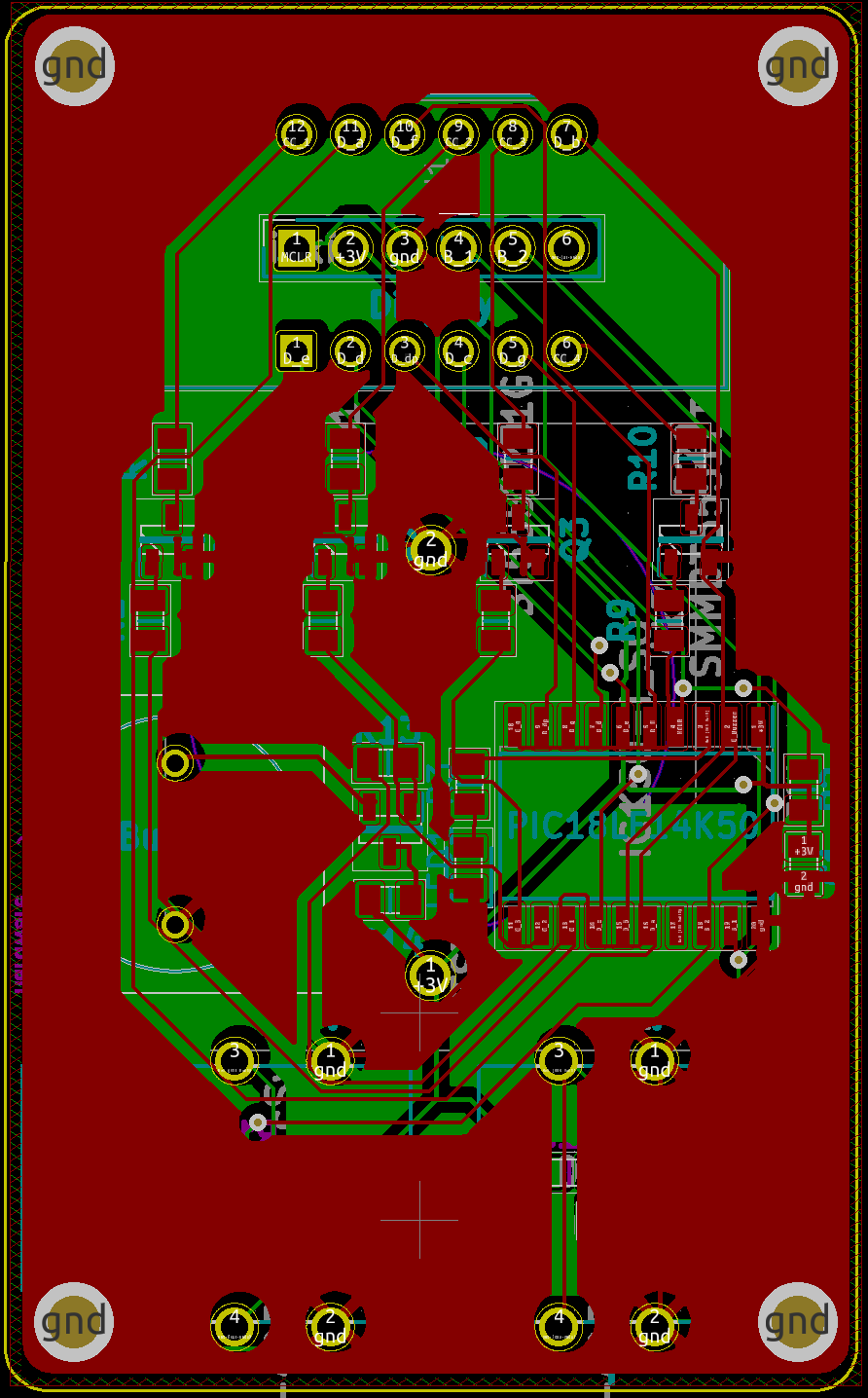
Finally, the PCB is filled with GND copper planes, and imported to KICAD again:
And now everything is ready for the PCB manufacturer
Discussions
Become a Hackaday.io Member
Create an account to leave a comment. Already have an account? Log In.