 David H Haffner Sr
From the specifications sheet for the JDEPC-05 cmos sensor;
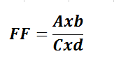
To find a theoretical MTF curve for a sensor, it is necessary to know three characteristics of the sensor: the active sensing area, the area comprising the sensing area and the interconnection and support structures ("real estate"), and the total number of those areas (the pixel count). The total pixel count is almost always given. Sometimes the overall sensor dimensions are given, from which the real estate area can be calculated. Whether the real estate area is given or derived, if the active pixel area is not given, it may be derived from the real estate area and the fill factor, where fill factor is the ratio of the active area to the dedicated real estate area;
 Where
Where
- the pixel real estate has dimensions c×d
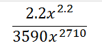
So in the case of the JDEPC-05 cmos sensor, our effective pixel area is; 3590 * 2710 um, this is our pixel “real estate,” our active area is 2.2um * 2.2um![]()
= 0.49 X 100= 49 % theoretical MTF from the table below, this is for a CCD detector but the resolution principle is the same. Row # 3 shows a horizontal pixel resolution of 1024 pixels and its corresponding resolution at the appropriate wavelength. Our wavelength is 532nm, so I will just recalculate this equation to fit my wavelength;![]()
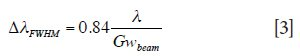
0.84 x 532/1540 x 4.8 = 1.39nm pixel resolution![]()
Process Raman typically requires ~10 cm-1 resolution, so with a 1024-pixel detector (4.5 cm-1/pixel sampling as seen from Table I) we should be able to obtain the required resolution.
*a quick note, the values in the table above refer to horizontal pixels, so in closing, the JDEPC-05 cmos sensor has 4.8 cm-1/1.39nm resolution @ 532nm, more than adequate for detecting Raman signals. - I also want to close with this thought, I have a poster of Einstein that I have had since I was in high school, and it is a quote of his; “The definition of genius is taking the complex and making it simple.”

Discussions
Become a Hackaday.io Member
Create an account to leave a comment. Already have an account? Log In.