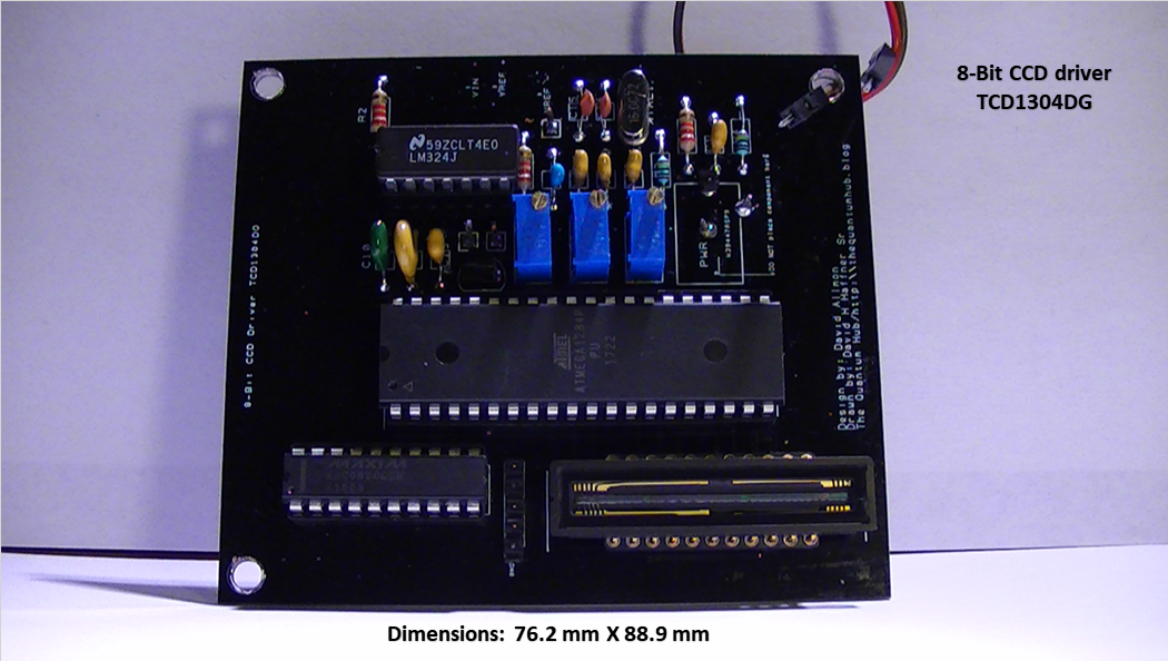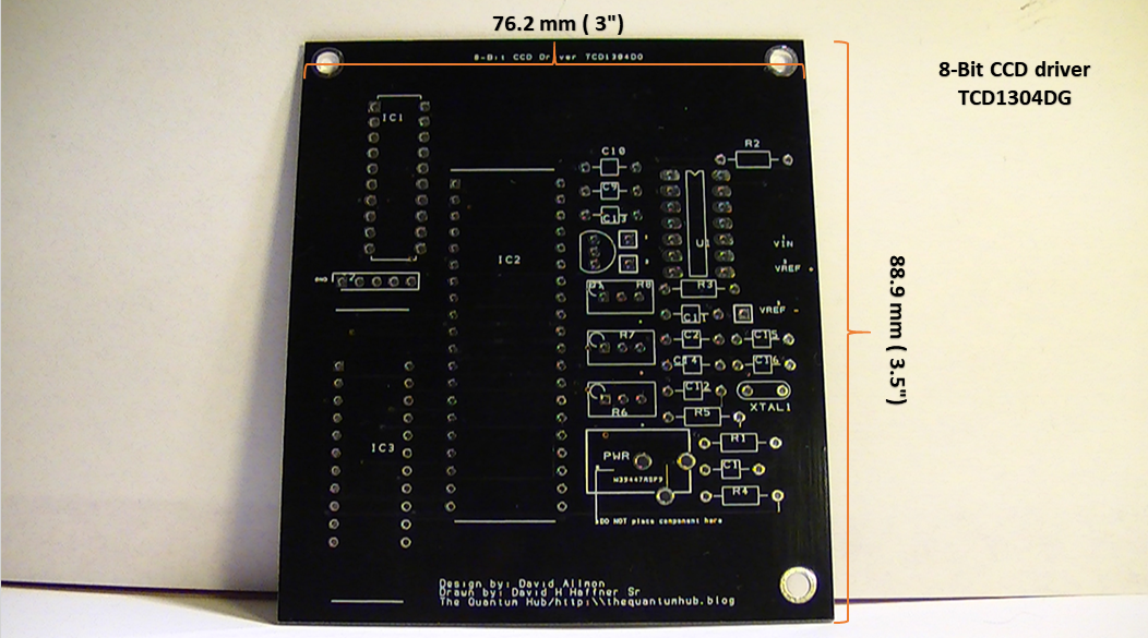
Final board design (needs 1 minor track change from C9 & C13 on PCB, could have been my fault upon manual component placement.) All in all, this baby works :)
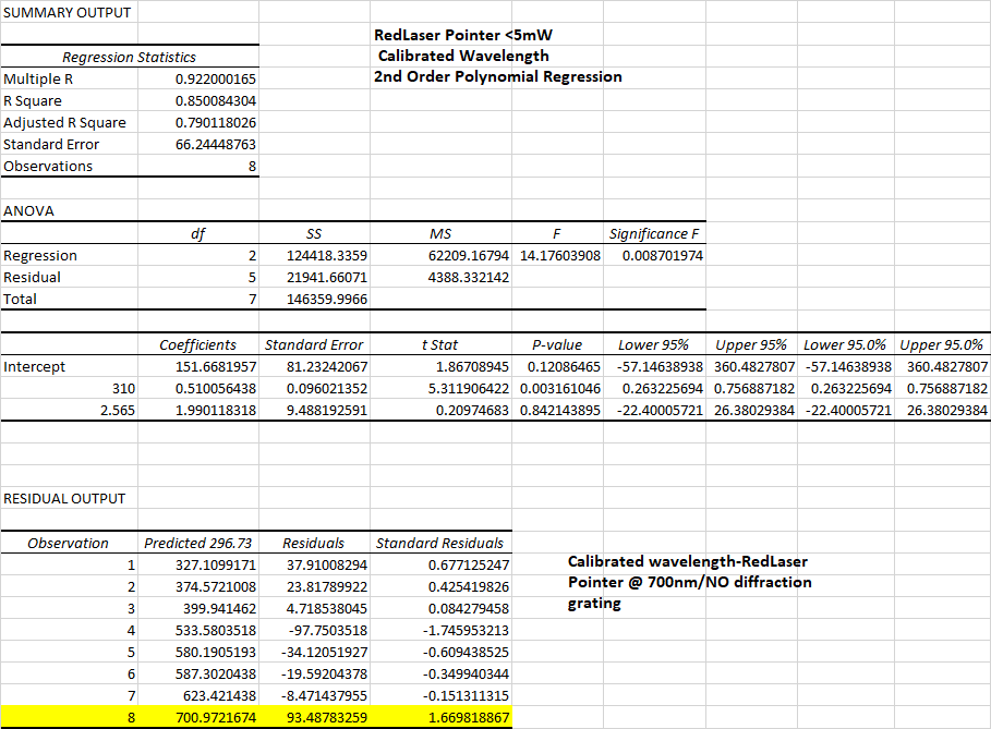
The plots below will show a red laser pointer (<5mW) aimed approx. center on the CCD, NO diffraction grating but I used a 2nd order regression formula table I made on Excel to calibrate the pixels into wavelength (nm).

This is the un-calibrated plot, it has been corrected for Intensity sensitivity (using an official data set from the Solux corp. technical website/Solux broadband spectrum-4700K ( 260 - 1100nm)

This is the summary output from Excel using 8 "true" wavelength peaks from an Hg calibrated lamp spectrum. The R squared value is not quite were it should be ( .999) but that's because there was no diffraction grating and I was holding the Laser pointer with my hand.
Still very close, this is just an initial example, making sure the circuit board is functional. The laser pointer states 650nm, but I am getting a calibration of 700nm, probably is about 650nm when I get it in the enclosure with all the optics in place, it should register normally.

This is the FWHM value data

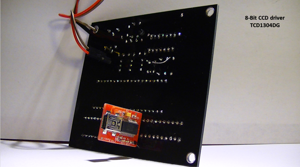
This is how I have the board designed so the USB cable enters the FTDI from the rear and power also enters from the rear and connects to the Arduino Mega 2560 mounted on the side of the enclosure.

Finally, a front view of the PCB, everything is tightly placed together, I found out something very interesting since this is the 5th re-design, the ADC does NOT like to be too close the LM324 (opamp) I'm sure I could have solved this problem if I would have taken a little more time and perhaps followed the recommended PCB design on the data sheet for the LM324 but it also required a low pass buffer and I just was not in the mood for so much work, sorry.
Anyway I am excited that it finally works well and can't wait to get it in the enclosure with all the fancy optics!
 David H Haffner Sr
Discussions
Become a Hackaday.io Member
Create an account to leave a comment. Already have an account? Log In.