 agp.cooper
Version 4
In version 4 I want to use a less aggressive memory write timing. Here is the updated Control logic:
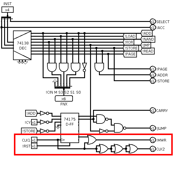
Here I have done two things:
- The system clock (CLK2) is delayed 18ns behind the clock input (CLK1).
- The Memory WRite signal is ORed the clock input.
The results for the Memory WRite (!MWR) timing are:
- tAS (Address Setup time) is about half a clock cycle.
- tWR (Write Recovery time) is about 27 ns (before the rise of CLK2)
Replacing the 74LS189
Replacing the 74LS189 with a standard Static RAM (SRAM) such as a 6116.
This requires a modification to the ALU to make the output tri-state and to directly select the Port bus:
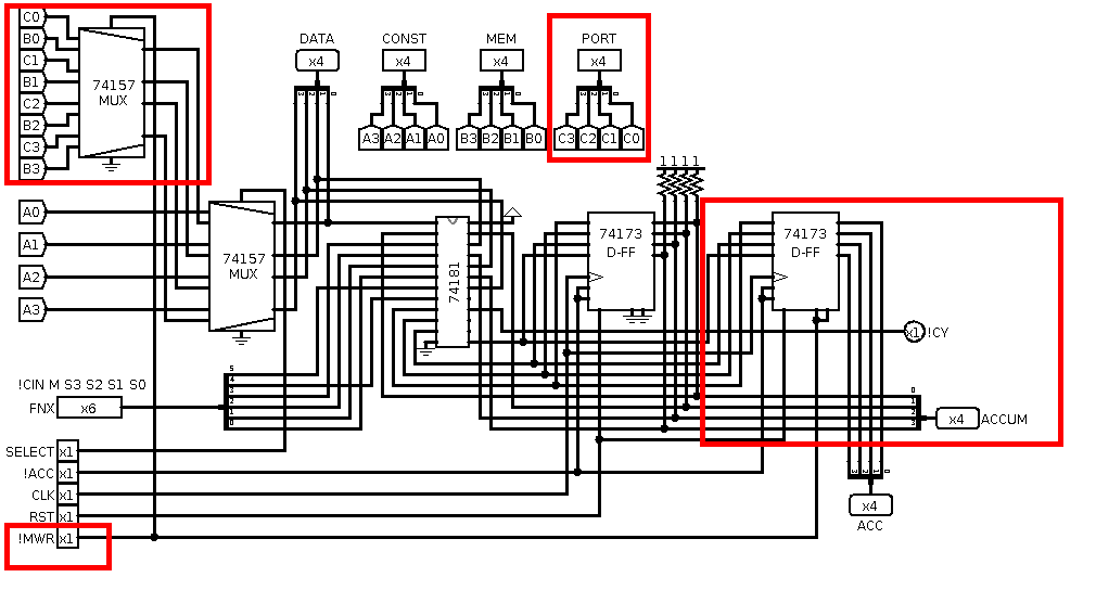
There is also a new ACCUM bus so that the Accumulator can be monitored regardless of the output state of the ACC bus.
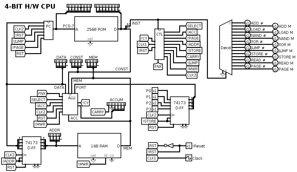
Here is the updated Top Level Schematic:
Upgrading the Clock
I want to upgrade the Reset and Step with Run (clock) and Stop (clock). The logic should be Reset and Step should stop the clock:
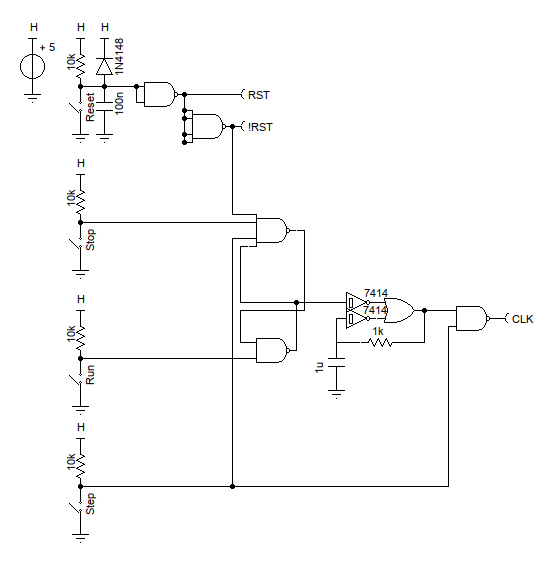
Note: I have added power on reset.
Note: The 7414/Or mess is actually one gate of a 74HC132 (Schmitt Trigger).
AlanX
Discussions
Become a Hackaday.io Member
Create an account to leave a comment. Already have an account? Log In.