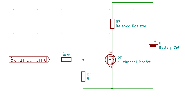
This was the first version of the balancing circuit diagram of cell module:

The balancing command digital output (from Attiny microcontroller) drives a N-channel Logic Mosfet which closes the circuit on the balancing resistor.
I did not like this version of the circuit for this reason: in the event of a short circuit failure between the source and drain of the mosfet, the circuit would have closed the resistance on the cell, causing the risk to damage the cell by falling below the minimum voltage threshold.
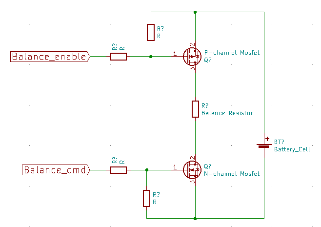
I wanted a protection for this event, so I modified the circuit like this:

I added a second P-channel Logic Mosfet on the positive power supply of the circuit, driven by another digital output of the microcontroller.
When the cell voltage is greater than 3200 mV, the balancing circuit is enabled, when it’s lower the balancing circuit is disabled.

So I protect the cell from the short circuit failure of the mosfet N, because below 3200 mV it is no longer balanced.
In the next evolution of the cell module, I decided to no longer drive the mosfet P from the microcontroller, but to use a hardware comparator circuit independent of the software of the microcontroller, in order to make the circuit even more safe.
 Sergio Ghirardelli
Discussions
Become a Hackaday.io Member
Create an account to leave a comment. Already have an account? Log In.